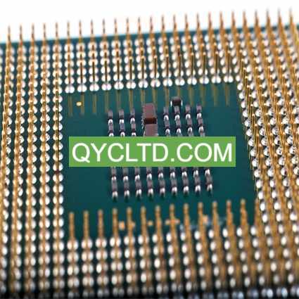
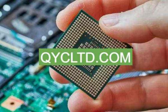
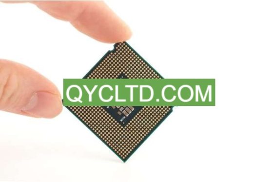
What is FCBGA Package Substrate?
FCBGA Package Substrate Manufacturer.FCBGA package substrate manufacturers specialize in crafting the intricate foundation for integrated circuits, ensuring reliability and performance in advanced electronic devices. Their expertise lies in fabricating substrates tailored to the demands of Flip-Chip Ball Grid Array (FCBGA) packages, crucial components in cutting-edge semiconductor technology. Employing precision engineering and innovative materials, these manufacturers produce substrates capable of supporting complex circuitry while optimizing thermal dissipation and signal integrity. Their commitment to quality and technological advancement underpins the seamless integration of semiconductor components, facilitating the development of next-generation electronics for diverse applications.
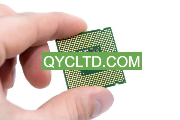
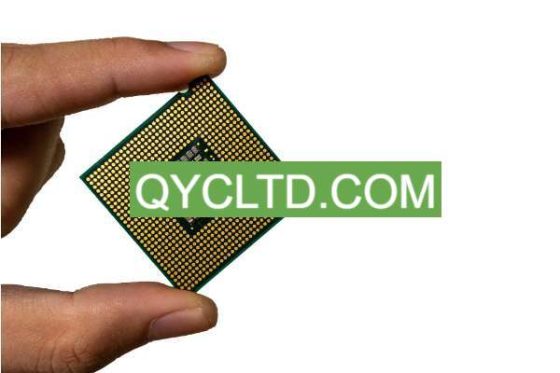
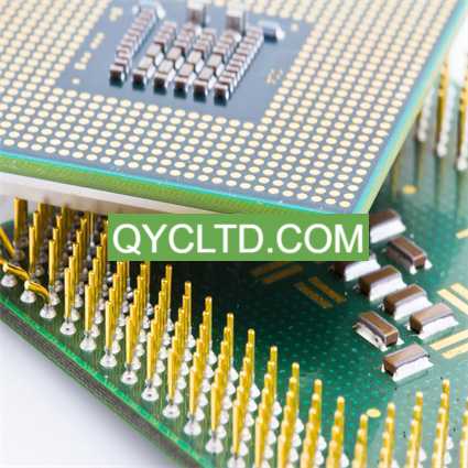
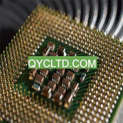
FCBGA, Flip Chip Ball Grid Array, is an advanced packaging technology widely used in the semiconductor industry. Different from the traditional wire bonding method, FCBGA uses flip-chip technology to directly connect the semiconductor chip to the พื้นผิวบรรจุภัณฑ์ through solder balls.
The traditional wire bonding method usually requires bonding the gold wire of the chip to the packaging substrate. This method may be limited by the length and resistance of the gold wire, affecting the speed and stability of signal transmission. FCBGA uses flip-chip technology, which inverts the chip and directly connects it to the packaging substrate, and the connection is achieved through solder balls. This method greatly reduces the path length of signal transmission and improves the speed and stability of signal transmission.
FCBGA packaging technology plays an important role in modern semiconductor packaging. It not only improves the density and performance of packaging, but also provides greater flexibility and reliability for the design and manufacturing of electronic products. Due to its unique design and advanced technology, FCBGA has been widely used in high-performance computing, อุปกรณ์สื่อสาร, industrial control, ยานยนต์อิเล็กทรอนิกส์และสาขาอื่น ๆ.
FCBGA Package Substrate design Reference Guide.
Designing an FCBGA requires extremely meticulous attention to detail. Substrate layout, via structure and routing configuration play a key role in ensuring signal integrity, thermal management and reliability. Engineers must follow industry standards and best practices to achieve optimal performance.
In FCBGA design, substrate layout is a crucial part. Reasonable substrate layout can ensure the stability and reliability of signal transmission. Good layout design can minimize signal interference and crosstalk and ensure the correct transmission of signals on the PCB. Engineers need to carefully plan the layout of devices to minimize signal path lengths and maintain sufficient distance between signal lines to reduce mutual interference.

FCBGA Package Substrate Manufacturer
The through-hole structure is also a part that requires special attention during the design process. Proper via design can effectively dissipate heat and provide pathways for signal transmission between different layers on the PCB. The location, size, and distribution of vias must be carefully considered based on specific application and layout requirements to ensure stable and reliable signal transmission.
นอกจากนี้, routing configuration is also one of the key steps in the design. Good routing design can optimize the signal transmission path to the greatest extent and reduce signal delay and distortion. Engineers need to pay attention to avoid crossover and interference between signal lines and adopt appropriate inter-layer wiring methods to ensure the reliability and stability of signal transmission.
When designing an FCBGA, engineers also need to pay close attention to thermal management. Due to the high integration level and high power consumption density of FCBGA packages, effective thermal management is crucial. Through reasonable heat dissipation design and thermal conduction path planning, the chip temperature can be effectively reduced and the stability and reliability of the system can be improved.
สรุป, designing FCBGA requires engineers to have comprehensive technical knowledge and rich experience. Through careful design of substrate layout, via structure and routing configuration, as well as effective thermal management strategies, FCBGA can be ensured to achieve optimal performance and reliability in various application scenarios.
What material is used in FCBGA Package Substrate?
The materials for FCBGA packaging usually use high-performance materials, such as laminates, organic substrates or advanced ceramics. These materials have excellent electrical properties, mechanical stability and thermal conductivity, which are critical for the reliable operation of electronic devices.
Laminate is a common FCBGA substrate material, consisting of multiple layers of resin substrate and copper foil. This material has excellent electrical properties, providing stable signal transmission and good impedance control. นอกจากนี้, the laminate also has good mechanical strength and can withstand the pressure and stress during the packaging process, ensuring the reliability of the packaging.
Organic substrate is another commonly used FCBGA substrate material, which is made of organic polymer substrate. This material has low dielectric constant and dielectric loss, which can reduce signal attenuation and crosstalk in signal transmission. ในเวลาเดียวกัน, organic substrates also have good processing properties and are suitable for the manufacturing of complex packaging structures.
In some high-performance applications, advanced ceramics are also used as materials for FCBGA substrates. This material has excellent thermal conductivity and mechanical strength, which can effectively dissipate heat and improve the reliability of the package. นอกจากนี้, advanced ceramics have good corrosion resistance and high temperature resistance, making them suitable for harsh working environments.
สรุป, the high-performance materials used in FCBGA packaging, including laminates, organic substrates and advanced ceramics, have excellent electrical properties, mechanical stability and thermal conductivity, providing a solid foundation for the reliable operation of electronic devices. The selection and application of these materials are critical to ensuring the performance and reliability of the FCBGA package.
What size are FCBGA Package Substrate?
FCBGA packages come in various sizes to accommodate different semiconductor chip sizes and pin counts. The size of the FCBGA package is determined by factors such as required floor space, wiring density and specific application requirements.
In electronic design, choosing the right size FCBGA package is crucial. ที่หนึ่ง, the size and number of pins of the semiconductor chip will directly affect the size of the package. เพราะฉะนั้น, the package must be sized to accommodate the chip and match the number of pins connected to it. Second, the required footprint depends on the application scenario. Some applications require a more compact package to save space, while other applications may require a larger package to accommodate more components or provide better heat dissipation capabilities.
นอกจากนี้, wiring density is also one of the important factors that determine the size of FCBGA. Designs with high routing density typically require larger packages to accommodate complex routing and more layers to ensure good signal integrity and electrical performance.
ในที่สุด, the requirements of specific application scenarios will also affect the size of the FCBGA package. เช่น, in some high-end computers or communications equipment, larger packages may be needed to accommodate larger processor chips or to support more high-speed interfaces.
สรุป, the size of the FCBGA package is a comprehensive consideration based on a variety of factors, including semiconductor chip size, pin count, wiring density and specific application requirements. Selecting the appropriately sized FCBGA package is critical to achieving optimal circuit performance and reliability.
The Manufacturing Process of FCBGA Package Substrate.
The manufacturing process of FCBGA (Flip Chip Ball Grid Array) involves multiple complex steps, including substrate manufacturing, chip attaching, packaging and ball attaching. The precision and high technical content of these steps ensure the precision, accuracy and consistency of producing high-quality FCBGA packages.
The first is substrate manufacturing, which is the first step in the FCBGA manufacturing process. Substrates are typically made from high-performance materials such as organic substrates or advanced ceramics. The manufacturing process of substrates requires precise process control to ensure that their size, flatness and electrical properties meet design requirements.
Next is chip attaching. ในขั้นตอนนี้, semiconductor chips are bonded to the substrate using a precise process. This involves treating the chip and substrate surfaces to ensure bonding reliability and good electrical connections.
Then comes packaging, a critical step that protects the chip and provides mechanical support. During the packaging process, the chip and substrate are covered with a protective material, usually epoxy resin. This layer of packaging material not only protects the chip from the external environment, but also provides solid mechanical support.
Finally comes the ball paste. ในขั้นตอนนี้, an electrical connection is made between the chip and the PCB by pasting molten solder onto the substrate. The pasting of these solder balls requires a high degree of precision and accuracy to ensure good electrical connection quality.
Throughout the manufacturing process, advanced manufacturing technologies such as precision control systems, automated assembly equipment and online quality monitoring systems play a key role. These technologies ensure the high quality and consistency of FCBGA packaging, thereby meeting the stringent performance and reliability requirements of modern electronic products.
Through these precise and complex manufacturing steps, the FCBGA package is able to achieve its excellent performance and reliability, providing a robust solution for a variety of application fields.
The Application area of FCBGA Package Substrate.
FCBGA package substrates are widely used in various industries, including telecommunications, computers, automobiles, อวกาศ, and consumer electronics. Its compact size, high pin density and excellent thermal performance make it ideal for applications requiring miniaturization, high-speed processing and reliability.
In the telecommunications industry, FCBGA package substrates are widely used in network equipment, base stations and communication equipment. Due to its miniaturization and high performance, FCBGA can meet the needs of telecommunications equipment for space efficiency and high-speed data transmission, providing important support for the development of communication networks.
In the computer field, FCBGA is commonly used in high-performance servers, data center equipment and embedded systems. Its high-density pin design and excellent thermal management capabilities enable it to cope with the needs of computing-intensive applications and provide stable and reliable performance.
In the automotive industry, FCBGA package substrates are widely used in automotive electronic control units (ECU), driver assistance systems and in-car entertainment systems. Its anti-vibration, high temperature resistance and strong reliability characteristics enable it to operate stably in harsh automotive environments, providing support for functional improvements and innovations in automotive electronic systems.
In the aerospace field, FCBGA plays an important role in avionics equipment, spacecraft control systems and navigation equipment. Its lightweight design and strong reliability enable it to meet the stringent weight and reliability requirements of aerospace equipment, providing key support for the advancement of aerospace technology.
ในด้านอุปกรณ์อิเล็กทรอนิกส์สําหรับผู้บริโภค, FCBGA is commonly used in products such as smartphones, แท็บ เล็ต, TVs, and game consoles. Its compact size and high-performance features enable it to meet consumer demands for portability, performance and user experience, promoting the continuous innovation and development of consumer electronics products.
สรุป, FCBGA package substrate plays an important role in various industries. Its excellent performance and versatility make it the first choice for various application scenarios, providing strong support for the development and progress of modern technology.
What are the advantages of FCBGA Package Substrate?
Improved electrical performance: FCBGA uses flip chip technology to make the interconnection length between the chip and the packaging substrate shorter, reducing parasitic effects and improving signal integrity and operation speed. This means devices can respond more quickly, transmit data at higher speeds, and provide users with a smoother experience.
Superior Thermal Management: Due to the flipped chip configuration, FCBGA is able to effectively dissipate heat, allowing electronic devices to handle power more efficiently and extending the life of the device. This advantage is particularly important in high-power-density applications such as high-performance computers, servers, and communications equipment.
Miniaturization: FCBGA has a compact packaging structure and high-density pin layout, making the design of electronic devices smaller and lighter. This allows us to design more portable smartphones, แท็บ เล็ต, portable medical equipment and other products to meet users’ needs for portability and lightweight.
Improved reliability: FCBGA provides strong mechanical and electrical connections through solder ball interconnects, greatly enhancing the durability and service life of the device. Compared with traditional wire bonding technology, solder ball interconnection is more reliable and can maintain stable performance under harsh environmental conditions.
สรุป, FCBGA, as an advanced packaging technology, not only has obvious advantages in electrical performance, thermal management, miniaturization and reliability, but also brings new possibilities and opportunities to the design and manufacturing of electronic devices. . ด้วยความก้าวหน้าอย่างต่อเนื่องของเทคโนโลยีและการขยายขอบเขตการใช้งาน, FCBGA will continue to play its important role and promote the development and innovation of the electronics industry.
คำถามที่ถามบ่อย
How does FCBGA compare to other packaging technologies in terms of cost?
FCBGA typically involves higher manufacturing costs compared to traditional packaging methods due to the complexity of the flip chip process and the use of advanced materials. อย่างไรก็ตาม, the benefits it offers in terms of performance, reliability, and miniaturization often justify the investment for many applications.
Can FCBGA packages be customized for specific applications?
Yes, FCBGA packages can be customized to meet the unique requirements of different applications. Engineers have the flexibility to tailor substrate designs, pin configurations, and thermal solutions to optimize performance and reliability for specific use cases.
What considerations should be taken into account when designing with FCBGA?
When designing with FCBGA, engineers must carefully consider factors such as signal integrity, การกระจายพลังงาน, thermal management, and manufacturability. Proper substrate layout, via placement, routing strategies, and thermal vias are critical to ensuring optimal performance and reliability.
Is FCBGA suitable for high-frequency applications?
Yes, FCBGA is well-suited for high-frequency applications due to its shorter interconnect lengths, reduced parasitic effects, and excellent signal integrity. It is commonly used in telecommunications, networking, and high-performance computing where high-speed data transmission is essential.
How does FCBGA facilitate thermal management?
FCBGA’s flip chip configuration allows for direct attachment of the semiconductor die to the package substrate, minimizing thermal resistance and enabling efficient heat dissipation. Additionally, advanced thermal management techniques such as heat spreaders, thermal vias, and thermal pads further enhance heat dissipation capabilities.
 ผู้ผลิตพื้นผิวแพ็คเกจเซมิคอนดักเตอร์
