What is FCCSP Package Substrate?
FCCSP Package Substrate Manufacturer.The FCCSP Package Substrate Manufacturer specializes in crafting cutting-edge substrates for advanced electronic packaging solutions. With a meticulous blend of innovative technology and precision engineering, they produce substrates that meet stringent industry standards. Their expertise lies in creating compact yet robust substrates tailored to accommodate diverse electronic components, ensuring optimal performance and reliability. Through continuous research and development, they remain at the forefront of the industry, offering clients customized solutions that seamlessly integrate with their specific requirements. As pioneers in their field, they redefine the benchmarks of quality and efficiency in electronic substrate manufacturing.
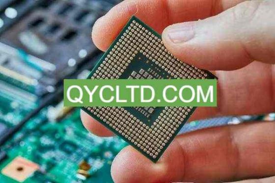
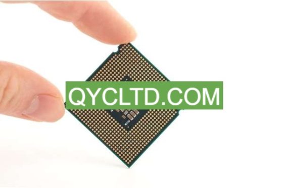
FCCSP Package Substrate (Flip Chip Chip Scale Package) is an innovative packaging technology designed to optimize the design and performance of electronic devices. This technology flips the chip over and tightly packages it on a printed circuit board (PCB), achieving a highly integrated and high-performance circuit layout. Compared with traditional packaging technology, FCCSP Package Substrate has outstanding advantages, mainly reflected in the following aspects:
First of all, FCCSP Package Substrate uses the chip’s flip packaging method to connect the chip directly to the PCB, reducing the length of wires required for traditional packaging, thereby reducing resistance and inductance, and improving signal transmission rate and performance stability. This direct connection design greatly reduces circuit delay and provides more stable and reliable support for high-speed circuits.
Secondly, FCCSP Package Substrate uses advanced packaging technology to package the chip in a very small size, achieving a highly integrated circuit layout. This compact packaging design not only saves space and makes electronic devices thinner and lighter, but also increases the density of circuit boards and increases the mounting density of electronic components, thus improving the functionality and performance of circuit boards.
In addition, the manufacturing process of FCCSP Package Substrate is relatively simple and the cost is relatively low. Compared with other high-end packaging technologies, FCCSP Package Substrate does not require complex manufacturing equipment and expensive materials, giving it a clear competitive advantage in mass production. This also provides electronic equipment manufacturers with more options to choose suitable packaging technology based on product characteristics and market demand to achieve a balance between cost and performance.

FCCSP Package Substrate Manufacturer
In summary, FCCSP Package Substrate, as an innovative packaging technology, has significant advantages and provides new possibilities for the design and manufacturing of electronic devices. With the continuous advancement of technology and the growing market demand, it is believed that FCCSP Package Substrate will play an increasingly important role in future electronic devices, bringing users a more convenient, efficient and stable experience.
FCCSP Package Substrate design Reference Guide.
Designing the FCCSP Package Substrate is a complex and critical task that involves many considerations to ensure that the stability, reliability and performance of the circuit board reach the expected level. The following are some design guidelines to help engineers better apply FCCSP Package Substrate technology in practice.
First, chip layout is one of the first considerations in the design process. When determining the layout of the chip, the physical connections of the circuit, signal transmission paths, and thermal design need to be considered. Reasonable layout can minimize signal interference and circuit noise, and improve system stability and performance.
Secondly, circuit connection is a crucial part of FCCSP Package Substrate design. Correct circuit connection design can ensure fast transmission and stability of signals and avoid failures caused by poor connections. Engineers need to carefully design the wiring of circuit connections and use appropriate connection methods, such as soldering or crimping, to ensure the connection is strong and reliable.
In addition, power consumption distribution is also one of the important factors that need to be considered during the design process. When designing the FCCSP Package Substrate, engineers need to reasonably plan power consumption distribution to avoid performance problems caused by local overheating or uneven power consumption. Through reasonable power consumption distribution design, the stability and work efficiency of the system can be improved and the service life of the equipment can be extended.
In addition to the above points, the design of FCCSP Package Substrate also needs to consider electromagnetic compatibility (EMC), anti-interference ability, mechanical strength and other factors. Engineers need to comprehensively consider various factors and take effective design measures to ensure that the circuit board can work normally in various working environments.
In short, designing FCCSP Package Substrate requires engineers to have deep professional knowledge and rich practical experience, and at the same time, multiple factors need to be considered comprehensively. Through reasonable design, the stability, reliability and performance of the circuit board can be ensured to reach the best level, thereby meeting the needs of different application scenarios.
What material is used in FCCSP Package Substrate?
The manufacturing process of FCCSP Package Substrate is a complex and precise process that requires multiple steps to ensure the quality and performance of the final product. These steps are detailed below:
Design of multi-layer PCB: The first step in manufacturing FCCSP Package Substrate is to design the multi-layer PCB. During the design stage, engineers need to consider factors such as chip layout, circuit connections, power consumption distribution, etc. to ensure the stability and reliability of the circuit board. The accuracy of the design phase directly affects the smooth progress of subsequent manufacturing and testing.
Chip flipping: Next comes the step of flipping the chip over and positioning it precisely on the PCB. This requires sophisticated equipment and technology to ensure that the chip is properly connected to the circuit board and that the connection is strong and reliable. During the process of flipping the chip, special attention needs to be paid to protecting the chip to avoid damaging the chip.
Soldering: Soldering is a critical step in connecting the chip to the circuit board. Welding processes, such as hot air soldering iron, hot plate crimping and other technologies, are usually used to connect the chip to the PCB. In this step, parameters such as temperature, pressure and time need to be controlled to ensure the quality and stability of the welding.
Testing: The last step is to test the manufactured FCCSP Package Substrate. Testing includes functional testing, electrical testing, reliability testing, etc. Testing can verify whether the product meets the design requirements and ensure that the quality and performance of the product meet customer expectations.
Throughout the manufacturing process, precise process control is the key to ensuring product quality. From PCB design to chip flipping to soldering and testing, every step needs to be strictly controlled and carefully adjusted to ensure the stability, reliability and performance of the final product. Only through a strict manufacturing process can high-quality FCCSP Package Substrate be produced to meet the ever-evolving needs of electronic equipment.
What size are FCCSP Package Substrate?
FCCSP Package Substrate is a key technology, and its material selection is crucial, directly affecting the performance, stability and reliability of the product. In the manufacturing of FCCSP Package Substrate, common materials include FR-4 (glass fiber reinforced epoxy resin), FR-5 and other high-performance materials such as polyimide (PI).
FR-4 is one of the most commonly used substrates with good mechanical and electrical properties and is widely used in PCB manufacturing. Its main components are glass fiber and epoxy resin, which are made through a lamination process. It has high strength and heat resistance and is suitable for various application scenarios.
Similar to FR-4, FR-5 is also a fiberglass reinforced epoxy material, but has slightly different properties. FR-5 has higher thermal stability and mechanical strength and is suitable for applications with high requirements for high temperature environments and high pressures, such as automotive electronics, aerospace and other fields.
In addition to FR-4 and FR-5, polyimide (PI) is another common FCCSP Package Substrate material. Polyimide has excellent high temperature stability, chemical stability and mechanical properties, and is suitable for high-end electronic equipment and applications in special environments, such as aerospace, military and other fields.
In addition, with the development of technology, some new high-performance materials have emerged, such as polyetheretherketone (PEEK), polystyrene (PS), polytetrafluoroethylene (PTFE), etc., which have better performance. It can meet the higher requirements for FCCSP Package Substrate in different fields.
To sum up, the material selection of FCCSP Package Substrate is a process that comprehensively considers various factors. Reasonable selection needs to be made based on specific application scenarios, performance requirements and cost considerations. Different materials have different characteristics and advantages, which can meet the design of electronic devices with various different needs.
The Manufacturing Process of FCCSP Package Substrate.
The size specification of FCCSP Package Substrate is one of the key considerations in the design and manufacturing process, because it directly affects the final size, performance and application scope of the circuit board. The flexibility of this packaging technology makes it suitable for a variety of chip sizes and circuit layouts, thus meeting the needs of a variety of small electronic devices.
First, the size of the FCCSP Package Substrate is usually closely related to the chip size. The size of the chip determines the minimum size of the package, so the most appropriate packaging solution needs to be determined based on the size of the chip during the design process. This compact packaging method allows the circuit board to accommodate more functional units, thereby improving the performance and functionality of the device.
Secondly, the complexity of the circuit will also affect the size of the FCCSP Package Substrate. For complex circuit layouts, larger package sizes may be required to accommodate more circuit components and connecting lines. Therefore, circuit complexity and space utilization efficiency need to be considered comprehensively during the design process to ensure that the package size can meet functional requirements without being too large.
Finally, application requirements are also one of the important factors that determine the size of the FCCSP Package Substrate. Different application scenarios may have different requirements for package size. For example, in mobile devices, smaller package sizes are often required due to limited space, while in industrial control equipment, larger package sizes may be required to accommodate more connectors and interfaces.
In general, the size of the FCCSP Package Substrate can be flexibly adjusted according to chip size, circuit complexity and application requirements. It can be as small as a few millimeters and is suitable for a variety of small electronic devices, including smartphones, tablets, smart wearables, medical devices, etc. Through reasonable design and manufacturing, FCCSP Package Substrate can achieve high-performance, high-reliability electronic products while maintaining a compact size.
The Application area of FCCSP Package Substrate.
FCCSP Package Substrate is widely used in various fields. Its high performance and small size make it the first choice for mobile devices, smart wearables, medical equipment, automotive electronics and other industries. Products in these fields have stringent requirements for size and performance, and FCCSP is an ideal choice to meet these requirements.
First, let’s look at the world of mobile devices. With the popularity of mobile devices such as smartphones and tablets, the requirements for circuit board size are getting higher and higher. The small size design of FCCSP Package Substrate makes it an indispensable part of devices such as mobile phones and tablets. It can not only provide higher performance, but also accommodate more functional modules in a limited space, providing users with a richer experience.
Secondly, the smart wearable field is also one of the important application fields of FCCSP Package Substrate. Products such as smart watches and health monitoring devices require compact and lightweight designs so that users can wear them comfortably. The small size and high performance of FCCSP Package Substrate make it an ideal choice for smart wearable devices, which can meet the functional requirements of the device in a limited space and maintain the thin and light design of the device.
In the field of medical devices, FCCSP Package Substrate also plays an important role. Medical devices have extremely high requirements for stability and reliability, and FCCSP Package Substrate can provide high-density circuit layout and stable performance, making it the preferred packaging technology for medical devices. From portable medical diagnostic equipment to implantable medical devices, FCCSP Package Substrate can bring more advanced solutions to the medical industry.
Finally, the automotive electronics field is also one of the important application fields of FCCSP Package Substrate. With the development of automobile intelligence and electrification, automotive electronic systems have increasingly higher requirements for size and performance. FCCSP Package Substrate can meet the high-performance requirements of automotive electronic systems in limited space and provides strong support for the development of automotive electronic systems.
In summary, FCCSP Package Substrate is widely used in mobile devices, smart wearables, medical devices, automotive electronics and other fields, providing higher performance and smaller size for products in these fields, and promoting the continuous development of related industries. and innovation.
What are the advantages of FCCSP Package Substrate?
The advantage of FCCSP Package Substrate is that it has many significant advantages compared with traditional packaging technology. These advantages make it the preferred packaging solution for today’s electronic equipment design. The following are the main advantages of FCCSP Package Substrate:
FCCSP Package Substrate uses advanced packaging technology to package chips into extremely small sizes. Compared with traditional packaging technology, it can reduce the overall size of the circuit board to a minimum, making electronic devices more compact and lightweight, meeting users’ needs for portability.
Due to the small size of the chip packaged by FCCSP Package Substrate, the circuit board material used is also lighter than traditional packaging technology. This not only reduces the overall weight of the electronic device, but also improves the portability and comfort of the device, making it more convenient for users to carry and use the device.
FCCSP Package Substrate uses a high-density, high-performance packaging process to integrate more functional modules and chips in a smaller size. This has resulted in significant improvements in the performance of electronic devices, including faster processing speeds, higher data transmission rates, and more stable performance, thereby meeting users’ needs for high-performance devices.
FCCSP Package Substrate can integrate multiple functional modules on a small-sized chip, thereby reducing the number of components and space occupied on the circuit board. This highly integrated design not only simplifies the layout and connection of the circuit board, but also improves the reliability and stability of the equipment and reduces the failure rate and maintenance cost of the circuit board.
To sum up, FCCSP Package Substrate, as an advanced packaging technology, has many advantages such as small size, light weight, high performance, and high integration, and can meet the continuous pursuit of size and performance of modern electronic equipment. With the continuous advancement of technology and the continuous expansion of application fields, it is believed that FCCSP Package Substrate will play an increasingly important role in future electronic device design, bringing users a more convenient, efficient, and intelligent product experience.
FAQ
What types of chips is FCCSP Package Substrate suitable for?
FCCSP Package Substrate is suitable for various types of chips, including processors, memory chips, sensors, etc. Whether it is a high-performance processor or a miniature sensor, FCCSP can provide stable and reliable packaging solutions.
How reliable is FCCSP Package Substrate?
FCCSP Package Substrate has been rigorously manufactured and tested and has excellent reliability and stability. Advanced processes and quality control measures are used in its manufacturing process to ensure that the product can operate stably for a long time in various application scenarios.
What is the manufacturing cost of FCCSP Package Substrate?
The manufacturing cost of FCCSP Package Substrate is relatively low, but the specific cost depends on factors such as material selection and design complexity. Compared with traditional packaging technology, the manufacturing process of FCCSP is more simplified, so it can effectively reduce manufacturing costs.
What are the advantages of FCCSP Package Substrate compared to other packaging technologies?
Compared with other packaging technologies, FCCSP Package Substrate has the advantages of small size, light weight, high performance and high integration. Its compact package enables higher chip density while improving board performance and reliability.
In what fields is FCCSP Package Substrate widely used?
FCCSP Package Substrate is widely used in mobile devices, smart wearables, medical equipment, automotive electronics and other fields. In these areas, the requirements for size and performance are very high, and FCCSP meets these requirements and becomes an ideal packaging choice.
What issues should be paid attention to when designing FCCSP Package Substrate?
When designing the FCCSP Package Substrate, special attention needs to be paid to issues such as chip layout, circuit connection, and heat dissipation design. Proper design can ensure the stability, reliability and performance of the circuit board.
 Semiconductor Package Substrate Manufacturer
