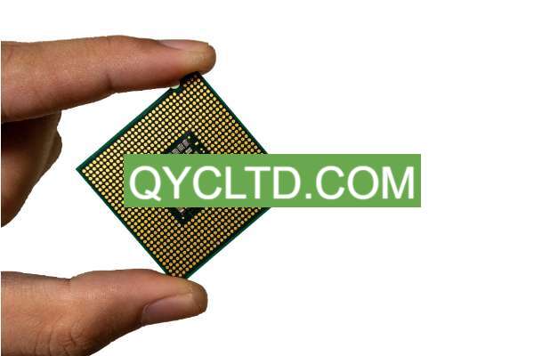
Ultra-Multilayer FCCSP (Flip Chip Chip Scale Package) substrates are advanced packaging solutions designed to support the increasing complexity and performance demands of modern electronic devices. These substrates feature multiple layers of circuitry, enabling high-density interconnects and efficient thermal management. Ultra-Multilayer FCCSP substrates are crucial in applications where miniaturization, high performance, and reliability are essential, such as in smartphones, high-performance computing, and telecommunications.
What is an Ultra-Multilayer FCCSP Substrate?
An Ultra-Multilayer FCCSP substrate is a type of semiconductor package substrate designed to support flip chip bonding and multiple layers of circuitry. The FCCSP technology involves mounting the semiconductor die face-down on the substrate, allowing for direct electrical connections between the die and the substrate via solder bumps. This packaging method reduces the package size and enhances electrical performance by minimizing the length of the interconnections.
이 “ultra-multilayer” aspect refers to the use of multiple layers of circuitry within the substrate. These layers enable high-density routing of signals and power, which is essential for supporting the complex and high-speed operation of modern semiconductor devices. Ultra-Multilayer FCCSP substrates provide improved signal integrity, efficient power distribution, and enhanced thermal management, making them ideal for high-performance applications.

Ultra-Multilayer FCCSP Substrates Manufacturer
Ultra-Multilayer FCCSP Substrate Design Reference Guide
Designing Ultra-Multilayer FCCSP substrates involves several critical considerations to ensure optimal performance and reliability. The following sections provide an overview of the key aspects involved in the design and application of these substrates.
The materials used in Ultra-Multilayer FCCSP substrates are selected for their superior electrical, thermal, and mechanical properties:
High-Performance Dielectric Materials: Advanced dielectric materials, such as polyimides and liquid crystal polymers, are used to provide excellent electrical insulation and support high-frequency signal transmission.
Copper: Ultra-thin copper layers are used for the conductive traces, offering excellent electrical conductivity and allowing for fine-line patterning necessary for high-density interconnects.
Solder Mask: A high-precision solder mask is applied to protect the underlying circuitry and prevent solder bridging during assembly. The solder mask must withstand the high temperatures of reflow soldering and other assembly processes.
Adhesives: Advanced adhesives are used to bond the layers together, ensuring mechanical stability and minimizing signal loss.
Several key considerations must be addressed during the design phase:
Impedance Control: Precise impedance control is essential for maintaining signal integrity, especially at high frequencies. This involves careful design of the signal traces and the use of controlled impedance materials.
Thermal Management: Effective thermal management is crucial for high-performance applications. The design must incorporate thermal vias, heat sinks, or other techniques to efficiently dissipate heat generated by high-power components.
Mechanical Stability: The substrate must provide robust mechanical support to withstand thermal cycling and mechanical stresses during operation.
Reliability: Long-term reliability is ensured through the use of high-quality materials and precise manufacturing processes, preventing issues such as delamination and warping.
What Materials are Used in Ultra-Multilayer FCCSP Substrates?
Materials used in Ultra-Multilayer FCCSP substrates are selected for their complementary properties to enhance the overall performance of the substrate:
High-Performance Dielectric Materials: Advanced dielectric materials provide electrical insulation and support high-frequency signal transmission.
Copper: High-purity copper is used for the conductive layers, offering excellent electrical conductivity and enabling fine-line patterning.
Solder Mask: A thin, high-precision solder mask protects the underlying circuitry and prevents solder bridging during assembly, withstanding the high temperatures of reflow soldering.
Advanced Adhesives: Specialized adhesives bond the layers together, providing mechanical stability and minimizing signal loss.
What Size are Ultra-Multilayer FCCSP Substrates?
The size of Ultra-Multilayer FCCSP substrates varies depending on the application and specific design requirements:
Thickness: The overall thickness of Ultra-Multilayer FCCSP substrates can range from a few hundred micrometers to over a millimeter, depending on the number of layers and the application requirements.
Dimensions: The length and width of the substrates are determined by the size of the components and the layout of the system. They can range from small form factors for compact devices to larger substrates for more complex electronic systems.
The Manufacturing Process of Ultra-Multilayer FCCSP Substrates
The manufacturing process of Ultra-Multilayer FCCSP substrates involves several precise and controlled steps to ensure high quality and performance:
High-quality base materials, such as copper-clad laminates and advanced dielectric materials, are selected and prepared for processing. The materials are cleaned and treated to remove any impurities and ensure a smooth surface.
The dielectric material is applied to the substrate in multiple layers, with each layer being patterned and cured to form the desired circuit patterns. This process is repeated to build up the required number of layers, ensuring high-density interconnects and excellent electrical performance.
Microvias and through-holes are drilled into the substrate to create electrical connections between the layers. These vias are then plated with copper to ensure reliable electrical conductivity and robust mechanical support.
The substrate surface is finished with a high-precision solder mask to protect the underlying circuitry and provide a smooth surface for component mounting. This step also includes the application of surface finishes, such as ENIG (Electroless Nickel Immersion Gold) or OSP (Organic Solderability Preservative), to enhance solderability and corrosion resistance.
After fabrication, the substrates are assembled with electronic components. Rigorous testing is conducted to ensure that the substrates meet all design specifications and performance requirements. This includes electrical testing, thermal cycling, and mechanical stress testing to verify the reliability and durability of the substrates.
The Application Area of Ultra-Multilayer FCCSP Substrates
Ultra-Multilayer FCCSP substrates are used in a wide range of high-performance electronic applications:
In consumer electronics, Ultra-Multilayer FCCSP substrates support high-performance and compact devices such as smartphones, 정제, 그리고 웨어러블 기술. The substrates provide the necessary electrical and thermal performance to ensure the reliable operation of these devices.
In medical devices, Ultra-Multilayer FCCSP substrates support high-frequency signal processing and reliable operation in various diagnostic and therapeutic equipment. These substrates ensure precise and accurate signal transmission, making them ideal for use in imaging systems, monitoring devices, and surgical instruments.
In automotive applications, Ultra-Multilayer FCCSP substrates are used in various electronic systems, including infotainment, navigation, and advanced driver-assistance systems (ADAS). These substrates offer high reliability and performance, enabling advanced functionalities and efficient operation in automotive environments.
In aerospace and defense applications, Ultra-Multilayer FCCSP substrates provide robust performance in harsh environments and under extreme conditions. These substrates are used in various aerospace and defense systems, such as radar, communication, and navigation systems, ensuring reliable operation and long-term durability.
In industrial automation, Ultra-Multilayer FCCSP substrates are used in various control and automation systems. These substrates offer high reliability and performance, enabling advanced functionalities and efficient operation in industrial environments.
What are the Advantages of Ultra-Multilayer FCCSP Substrates?
Ultra-Multilayer FCCSP substrates offer several advantages that make them indispensable in high-performance electronic applications:
High Performance: Ultra-Multilayer FCCSP substrates provide high-speed signal processing and excellent signal integrity, making them ideal for advanced electronic devices and systems.
Miniaturization: These substrates enable the integration of complex circuitry in a compact form factor, supporting the trend towards smaller and more powerful electronic devices.
Thermal Management: These substrates offer enhanced thermal management, efficiently dissipating heat generated by high-power components and ensuring reliable operation.
Reduced Warpage: The use of advanced materials and precise manufacturing processes reduces the risk of warpage, improving the mechanical stability and reliability of the substrate.
Reliability: Ultra-Multilayer FCCSP substrates provide robust mechanical support, efficient thermal management, and long-term reliability, ensuring the stable operation of electronic devices.
Versatility: Ultra-Multilayer FCCSP substrates can be used in a wide range of applications, from consumer electronics and medical devices to automotive and aerospace, providing advanced functionality and reliability in demanding environments.
자주 묻는 질문(FAQ)
What are the key considerations in designing an Ultra-Multilayer FCCSP substrate?
Key considerations include material properties, layer stack-up, 임피던스 제어, 열 관리, and mechanical stability. The design should ensure optimal electrical performance, efficient heat dissipation, and long-term reliability.
How do Ultra-Multilayer FCCSP substrates differ from traditional FCCSP substrates?
Ultra-Multilayer FCCSP substrates feature multiple layers of circuitry, enabling high-density routing and enhanced electrical performance compared to traditional FCCSP substrates, which may have fewer layers and lower density interconnects.

 반도체 패키지 기판 제조업체