What is IC/BGAパッケージ基板?
IC/BGA Package Substrate Manufacturer.As an IC/BGA package substrate manufacturer, we specialize in crafting the backbone of modern electronics. Our expertise lies in producing intricate substrates that provide the essential foundation for integrated circuits and ball grid arrays (BGAs). With meticulous attention to detail and cutting-edge technology, we engineer substrates that ensure optimal electrical connectivity and thermal management. Our commitment to quality and innovation drives us to constantly refine our processes, delivering substrates that meet the rigorous demands of the electronics industry. Trust us to be your reliable partner in building the next generation of electronic devices.
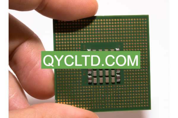
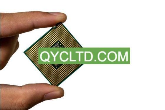
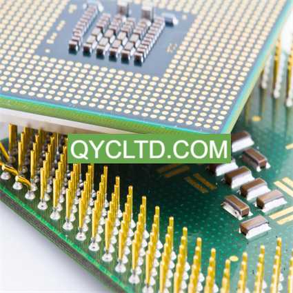
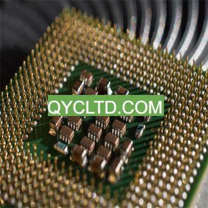
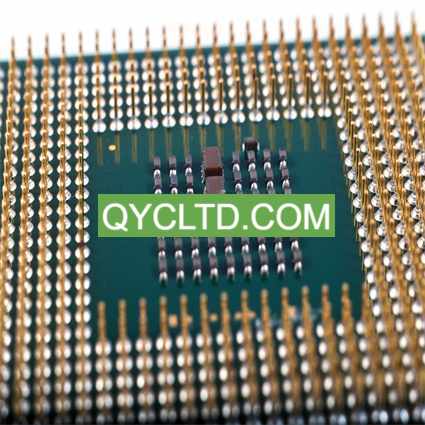
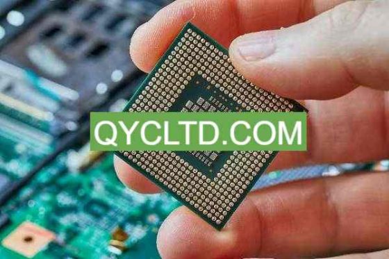
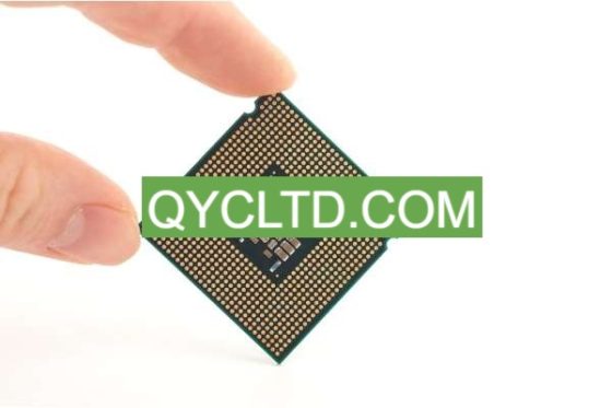
IC/BGA パッケージ基板 (Integrated Circuit/Ball Grid Array Package Substrate) is a PCB (Printed Circuit Board) form that integrates multiple chip packages. Its design integrates Ball Grid Array (BGA) packaged chips, which are usually integrated circuits (ICs) or other devices. IC/BGA Package Substrate is widely used in modern electronic products, including smartphones, 錠剤, computers, and other embedded systems.
Smartphones are a typical example of IC/BGA Package Substrate applications. In a typical smartphone, IC/BGA Package Substrate achieves a high degree of integration and functional density by integrating multiple chip packages on a PCB. These chips usually include processors, memory, graphics processors, communication modules, 等. By integrating multiple functional units in a compact space, IC/BGA Package Substrate can achieve higher performance and smaller size, thereby meeting the growing performance needs of smartphones and the requirements for thin and light designs.
Similarly, IC/BGA Package Substrate is widely adopted in tablets and computers. In these devices, IC/BGA Package Substrate not only realizes the integration of chip packaging, but also provides high-speed, high-density circuit connections for the devices to meet the requirements of complex circuits and high-speed data transmission. さらに, IC/BGA Package Substrate can also provide better thermal management and help the device maintain good heat dissipation performance, thus improving the reliability and stability of the device.

IC/BGAパッケージ基板メーカー
Embedded systems are another typical application field, and IC/BGA Package Substrate plays a key role in these systems. Embedded systems often require highly integrated circuit designs to meet performance, power consumption, and size requirements. IC/BGA Package Substrate provides a highly flexible solution for embedded systems by integrating multiple functional units on a compact PCB, allowing designers to achieve more functions, smaller size and lower power consumption .
原則として, IC/BGAパッケージ基板, as a highly integrated PCB form, plays a key role in modern electronic products. By integrating multiple chip packages, it achieves the design goals of high performance, small size, and low power consumption, providing important support and driving force for the development of electronic products.
IC/BGAパッケージ基板 design Reference Guide.
When designing IC/BGA Package Substrate, engineers need to consider many factors, such as circuit layout, stacking method, シグナルインテグリティ, 等. To ensure high performance and reliability, designers should follow PCB design guidelines, which usually include information on routing rules, pin layout, ground and power plane planning.
Routing rules refer to the guidelines for how to place and connect circuit components in PCB design. This includes the wiring path, スペーシング, wiring method, 等. of signal lines and power lines. Reasonable wiring rules can reduce signal interference and improve signal integrity, thereby ensuring circuit performance and stability.
In IC/BGA Package Substrate design, pin layout is crucial. Designers need to consider the pinout of individual devices to minimize signal delays, reduce crosstalk, and ensure good connections to signal and power lines.
Ground and power plane planning refers to how to design the ground and power layers in the inner layout of the PCB board. Good ground and power plane planning can effectively reduce electromagnetic interference, provide stable power supply, and ensure the reliability and stability of the entire circuit.
Signal integrity refers to maintaining the accuracy and integrity of the signal during signal transmission. In order to ensure signal integrity, designers need to consider factors such as signal line length matching, インピーダンス整合, and grounding methods between the signal layer and the ground plane to reduce signal reflection, crosstalk, and timing skew.
By following the above PCB design guidelines, engineers can better design IC/BGA Package Substrate to ensure its high performance and reliability. Reasonable circuit layout, pin layout, ground and power plane planning, and signal integrity design will provide strong support for the performance improvement and stable operation of electronic products.
What material is used in IC/BGAパッケージ基板?
IC/BGA Package Substrate is a key component of modern electronic design, and its material selection is crucial, directly affecting the performance, reliability and cost of PCB. The following will introduce the commonly used materials of IC/BGA Package Substrate and their characteristics and applications.
FR-4 is one of the most common PCB substrate materials and is also commonly used in the manufacturing of IC/BGA Package Substrate. It has excellent insulation properties, mechanical strength and heat resistance, making it suitable for most applications. FR-4 has a relatively low material cost and mature manufacturing process, so it is very popular.
High TG FR-4 is an improved FR-4 material with a higher glass transition temperature (TG value), usually above 150 degrees Celsius. This makes high TG FR-4 have better stability and durability in high temperature environments, making it suitable for applications that require working in high temperature environments, such as automotive electronics, industrial control and other fields.
Polyimide is a high-performance engineering plastic with excellent high temperature resistance, chemical resistance and mechanical strength. When IC/BGA Package Substrate uses polyimide as the substrate material, it can meet the requirements for high frequency, high speed and stability, and is suitable for communications, aerospace and other fields.
Copper-based substrate is a substrate material. The base material is usually metallic copper and the surface is covered with an insulating layer. It is suitable for high-power and high-heat electronic equipment. When the IC/BGA Package Substrate uses a copper-based substrate, it can effectively dissipate heat and improve the stability and reliability of the circuit. It is suitable for LED lighting, power modules and other fields.
For applications requiring higher frequencies, IC/BGA Package Substrate may use high-frequency dielectric materials, such as PTFE (ポリテトラフルオロ エチレン), RO4003C, 等. These materials have low dielectric constant, low loss factor and excellent high-frequency characteristics, can meet the requirements of high-speed transmission and signal integrity, and are suitable for radio frequency communications, radar systems and other fields.
Material selection for IC/BGA Package Substrate is critical to the success of electronic design. Designers should select appropriate materials based on the requirements of specific applications to ensure that the PCB has good performance, reliability and cost-effectiveness. By understanding the characteristics and application scenarios of various materials, designers can better utilize IC/BGA Package Substrate to drive future electronic innovation.
What size are IC/BGAパッケージ基板?
The size of IC/BGA Package Substrate is one of the crucial considerations in the design and application process. Its size not only affects the layout and shape of the circuit board, but is also directly related to the size, performance and heat dissipation effect of the device. When designing IC/BGA Package Substrate, engineers need to consider various factors to ensure optimal performance and reliability.
The size range of IC/BGA Package Substrate is quite wide and can vary according to specific application requirements. From chips of a few millimeters in micro electronic devices to chips of tens of centimeters in industrial applications, the size of the IC/BGA Package Substrate can be very flexibly adapted to different scenarios.
The size of the IC/BGA Package Substrate has high design flexibility and can be adjusted according to the specific circuit layout and component arrangement. This design flexibility allows engineers to maximize circuit layout optimization, improve signal integrity, and achieve optimal performance in limited space.
The size of the IC/BGA Package Substrate directly affects the heat dissipation effect. Larger size usually means more heat dissipation surface area, which can remove heat more effectively, thus improving the stability and reliability of the device. そこで, when designing IC/BGA Package Substrate, engineers usually consider heat dissipation requirements and select appropriate sizes to meet these requirements.
The size of the IC/BGA Package Substrate also directly affects its performance characteristics. Larger size usually means more wiring space and higher integration, which can accommodate more functional modules and devices, thereby improving the performance and functionality of the device. そこで, when designing IC/BGA Package Substrate, engineers need to make a trade-off between size and performance and find the best balance point.
In order to promote the design and manufacturing of IC/BGA Package Substrate, the industry usually establishes some size standards. These standards help engineers design and lay out circuit boards more easily and ensure that chips and packages produced by different manufacturers can be used interchangeably. Standardized dimensions also help reduce design and manufacturing costs and accelerate product time to market.
The size of IC/BGA Package Substrate is one of the crucial considerations in the design and application process. Engineers should take full advantage of their design flexibility and select the most appropriate size based on thermal requirements and performance needs to achieve the best circuit layout and performance. 同時に, the industry-standardized size also facilitates the design and manufacturing of IC/BGA Package Substrate, promoting the rapid development and popularization of electronic products.
The Manufacturing Process of IC/BGAパッケージ基板.
The manufacturing process of IC/BGA Package Substrate is a complex and precise engineering process, which involves multiple steps and processes and requires careful design and operation by engineers. The main steps of this process are detailed below:
Design stage: Before manufacturing the IC/BGA Package Substrate, engineers first need to perform detailed design work. This includes determining circuit layout, pin connections, ground and power plane planning, 等. Use computer-aided design (CADの) software to design graphically, taking into account factors such as signal integrity, thermal management, and EMI/EMC.
材料の選択: During the manufacturing process, engineers need to select the appropriate substrate material and copper thickness. Commonly used substrate materials include FR-4, FR-5, 等。, and the copper thickness is determined according to the circuit requirements and design specifications.
Printing: まずは, a layer of photosensitive agent is coated on the substrate, and then the PCB design pattern is transferred to the photosensitive layer through photolithography technology. Afterwards, the parts not covered by photolithography are chemically etched to remove unnecessary copper foil and form the desired circuit pattern.
Electroplating: After the circuit pattern is formed, the exposed copper foil surface needs to be electroplated to increase conductivity and corrosion resistance. Commonly used electroplating methods include electroless copper plating (Electroless Copper Plating) and electrolytic copper plating (Electroplating).
Etching: 次に, the copper foil not covered by the photosensitive layer is removed by chemical etching, leaving only the designed circuit pattern. After etching, it is cleaned and processed again to remove residual chemicals.
Soldering: After completing the circuit pattern production, the PCB needs to be soldered. This involves connecting the required components to the PCB using soldering techniques such as surface mount technology (SMT) or plug-in soldering technology.
Assembly and testing: 最終的に, the assembly process includes mounting IC/BGA packaged chips, other devices, connectors and other components onto the PCB and soldering them. Afterwards, functional testing, performance testing and reliability testing are performed to ensure that the quality and performance of the IC/BGA Package Substrate meet the design requirements.
Through these precise manufacturing steps, engineers are able to produce high-performance, reliable IC/BGA Package Substrate, which provides a solid foundation for the manufacturing and application of various electronic devices.
The Application area of IC/BGAパッケージ基板.
As a key PCB form, IC/BGA Package Substrate is widely used in various electronic devices, providing strong support for device performance, power consumption and reliability in these fields. The following will introduce in detail the application of IC/BGA Package Substrate in the fields of communication equipment, consumer electronics, medical equipment and automotive electronics.
In the field of communication equipment, IC/BGA Package Substrate plays a vital role. From smartphones to base station equipment, as well as routers and switches in communication networks, IC/BGA Package Substrate is widely used. These devices require high-performance, high-density circuit boards to support complex communication protocols and high-speed data transmission. The integration and signal integrity of IC/BGA Package Substrate make it an ideal choice for these devices.
The consumer electronics market is another important area for IC/BGA Package Substrate applications. From smart TVs to game consoles to smart home devices and audio systems, consumer electronics are increasingly demanding small, lightweight, and high-performance products. IC/BGA Package Substrate enables these devices to implement more complex functions and achieve higher performance and reliability in a smaller space by providing highly integrated solutions.
In the field of medical devices, IC/BGA Package Substrate is critical to support medical monitoring, diagnostic and treatment equipment. 例えば, devices such as pacemakers, medical imaging equipment, and patient monitoring systems require highly reliable electronic components to ensure patient safety and health. The high integration and reliability of IC/BGA Package Substrate make it the first choice for these medical devices.
With the continuous development of automotive electronic systems, IC/BGA Package Substrate is also playing an increasingly important role in the field of automotive electronics. Modern cars are equipped with many advanced electronic systems, such as engine control units, airbag systems, in-car entertainment systems, 等. These systems require high-performance, durable electronic components to ensure the safety and performance of the car. IC/BGA Package Substrate provides key support for the development of automotive electronic systems by providing highly integrated and highly reliable solutions.
原則として, IC/BGA Package Substrate plays a key role in communication equipment, consumer electronics, medical equipment, and automotive electronics. Their applications not only provide performance, power consumption and reliability support for devices in these fields, but also promote the continuous progress and innovation of electronic technology.
What are the advantages of IC/BGAパッケージ基板?
IC/BGA Package Substrate does have many significant advantages over traditional PCBs, and these advantages are critical to the design and performance of many high-performance electronic products.
まずは, IC/BGA Package Substrate has a higher level of integration. Because it integrates multiple chip packages, it can accommodate more functions and components in a smaller space. This highly integrated design can significantly reduce the size of electronic products and improve the overall performance of the system.
第二に, IC/BGA Package Substrate has better signal integrity. Through careful design and optimized layout, interference and loss in signal transmission can be minimized, thereby improving signal stability and reliability. This is critical for high-frequency, high-speed and high-performance electronics such as communications equipment and computers.
さらに, IC/BGA Package Substrate has smaller size and weight. Compared to traditional PCBs, IC/BGA Package Substrates are generally more compact and lightweight, making them ideal for applications that require small size and light weight, such as portable electronic devices and embedded systems.
Most importantly, IC/BGA Package Substrate has higher reliability. Because its design and manufacturing processes have been carefully optimized and verified, IC/BGA Package Substrate generally exhibits better stability and durability in the face of challenges and environmental changes. This means that electronic products can maintain stable and reliable performance over long periods of use and in various application environments.
まとめ, IC/BGA Package Substrate has become the first choice for many high-performance electronic products due to its higher integration, better signal integrity, smaller size and weight, and higher reliability. As the electronics industry continues to develop and technology advances, IC/BGA Package Substrate will continue to play an important role and promote the innovation and development of future electronic products.
FAQ
What are the advantages of IC/BGA Package Substrate compared with traditional PCB?
IC/BGA Package Substrate has multiple advantages over traditional PCB. 最初です, IC/BGA Package Substrate integrates multiple chip packages, which can achieve higher integration and reduce the size and weight of the circuit board. 第二に, because the chip package is more compact, IC/BGA Package Substrate performs better in high-frequency and high-speed applications and has better signal integrity. さらに, the manufacturing process of IC/BGA Package Substrate is more complex, but it can also achieve higher precision and reliability, and is suitable for areas with higher product performance requirements.
What application scenarios is IC/BGA Package Substrate suitable for?
IC/BGA Package Substrate is suitable for a variety of high-performance electronic device application scenarios. They are widely used in communication equipment, consumer electronics, computers, medical equipment, automotive electronics and other fields. In these fields, IC/BGA Package Substrate is particularly suitable for products with higher requirements in terms of integration, performance, reliability and volume.
What is the manufacturing cost of IC/BGA Package Substrate?
The manufacturing cost of IC/BGA Package Substrate is usually higher than that of traditional PCB. This is because IC/BGA Package Substrate requires more complex manufacturing processes, such as microscopic inspection, multi-layer stacking, high-density wiring, 等。, as well as higher-level substrate materials. さらに, since IC/BGA Package Substrate usually integrates multiple chip packages, the cost of assembly and testing will also increase. しかし, despite higher manufacturing costs, the performance and reliability advantages brought by IC/BGA Package Substrate can often make up for this gap, thus providing key support for the manufacturing of high-end electronic products.
What is the difference between IC/BGA Package Substrate and traditional PCB?
IC/BGA Package Substrate is a PCB form that integrates multiple chip packages and is typically used in high-performance and high-density applications. 従来のPCBとの比較, IC/BGA Package Substrate has higher integration and performance. They integrate multiple chip packages, such as Ball Grid Array (BGA), which makes it possible to integrate more functions and devices on the same board. さらに, IC/BGA Package Substrate usually has better signal integrity and electromagnetic compatibility, and can meet more stringent design requirements.
What applications is IC/BGA Package Substrate suitable for?
IC/BGA Package Substrate is suitable for a variety of high-performance electronic devices, including but not limited to smartphones, 錠剤, computers, communication equipment, medical equipment, and automotive electronics. They can provide highly integrated, high-performance and high-reliability solutions in these applications to meet the needs of electronic products in different industries.
 半導体パッケージ基板メーカー
