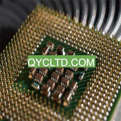
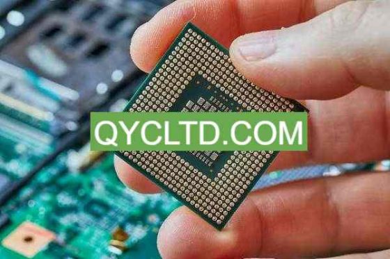
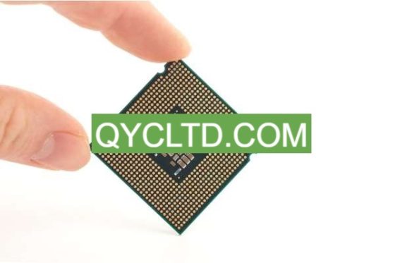
What is SIP Package Substrate?
SIP Package Substrate Manufacturer.The SIP Package Substrate Manufacturer specializes in crafting substrates tailored for System in Package (SIP) solutions. With meticulous precision, they engineer substrates to meet diverse technological demands, Gewährleistung optimaler Leistung und Zuverlässigkeit. Employing cutting-edge materials and advanced manufacturing techniques, they produce substrates that seamlessly integrate various components within compact packages. Their expertise lies in customizing substrates to accommodate specific chip sizes, configurations, and thermal requirements, empowering electronic devices with efficient connectivity and functionality. Renowned for their innovation and quality, they are the preferred choice for businesses seeking robust SIP solutions.
SIP package substrate, the full name is System-in-Package Verpackungs-Substrat, is an advanced form of integrated circuit packaging. It marks a departure from traditional PCB (printed circuit board) design by integrating multiple integrated circuits (Ik), passive components and interconnects into a single substrate.
Traditional PCB design usually treats the circuit board as a platform that holds and connects various components. Aber, the SIP package substrate integrates more functions into a smaller space, which means it can achieve higher functional density within a relatively small physical size.
The design of SIP package substrate is a complex and challenging task. It requires designers to consider how to lay out multiple components in a limited space and ensure that the interconnection paths between them are as short and reliable as possible. Außerdem, given the high integration and packaging density, thermal management has also become critical to ensure that components maintain a stable temperature during operation.
Material selection for this form of packaging is also critical. Common materials include high-performance polymers, ceramics, and metals, all of which have excellent electrical properties, mechanical stability, and thermal conductivity and are suitable for different application scenarios.
Insgesamt, SIP packaging substrates represent the latest advancement in modern integrated circuit packaging technology. By integrating multiple functions into a single substrate, it provides greater flexibility and freedom in the design of electronic devices, making it possible to achieve higher performance and more functions in a limited space.
SIP Package Substrate design Reference Guide.
Designing SIP package substrates requires a thorough understanding of layout considerations, signal integrity principles, thermal management strategies, and manufacturing feasibility constraints. Designers must optimize routing, reduce signal interference, and ensure compatibility with various manufacturing processes.
When designing a SIP package substrate, layout considerations are critical. Designers need to consider the layout between components to minimize signal path length and reduce signal propagation delay. Außerdem, the layout should also take into account factors such as power distribution, ground design, and pin assignments to ensure the stability and performance of the board.
Signal integrity is another important consideration in the design process. Designers must carefully choose the placement and routing of signal pins to minimize signal crosstalk and clock skew. By adopting appropriate signal pin layout and impedance matching techniques, signal integrity issues can be effectively reduced and system reliability and stability ensured.
Thermal management is an aspect that cannot be ignored in the design process. Multiple components are integrated into the SIP package substrate, so a large amount of heat is generated during operation. Designers need to adopt effective thermal management strategies, including rational layout of heat sinks, optimizing air flow and selecting appropriate heat dissipation materials, to ensure the stability and reliability of the system in high-temperature environments.
Endlich, designers must also consider manufacturing feasibility constraints. They need to understand the impact of different manufacturing processes on the design and ensure that the design meets the requirements of the manufacturing process. Zum Beispiel, designers may need to adjust component layout or modify routing paths to accommodate a specific manufacturing process and equipment.

SIP Package Substrate Manufacturer
Zusammenfassend, designing a SIP packaging substrate requires designers to comprehensively consider multiple aspects such as layout, Signalintegrität, Thermomanagement, and manufacturing feasibility. Only by fully understanding these factors can designers design SIP packaging substrates that are stable, zuverlässig, and have superior performance to meet the needs of various application fields.
What material is used in SIP Package Substrate?
SIP packaging substrates use a variety of materials, including high-performance polymers, ceramics and metals. These materials have excellent electrical properties, mechanical stability and thermal conductivity, ensuring reliable operation in harsh environments.
High-performance polymer is one of the important materials for SIP packaging substrate. They have excellent electrical insulation properties and can effectively isolate signals in the circuit and reduce signal interference. Außerdem, high-performance polymers also have good chemical stability and wear resistance, and can operate stably for a long time under harsh working conditions.
Ceramic materials play an important role in SIP packaging substrates. Due to their excellent thermal conductivity and high temperature resistance, ceramic materials are often used to deal with the heat dissipation problems of high-power electronic devices. Außerdem, ceramic materials also have good mechanical strength and chemical stability, which can ensure the stability and reliability of circuits in extreme environments.
Metal materials also play an important role in SIP packaging substrates. Metal materials are usually used to make conductor layers and connectors of electronic devices. They have good electrical conductivity and mechanical strength, and can ensure stable transmission of signals in circuits and reliability of connections. Außerdem, metal materials also have good thermal conductivity, which can effectively disperse the heat generated in the circuit and improve the heat dissipation effect of the system.
Zusammenfassend, the various materials used in SIP packaging substrates play an important role together to ensure the reliable operation of electronic devices in various harsh environments. These materials have excellent properties in terms of electrical properties, mechanical stability and thermal conductivity, laying a solid foundation for the high performance and reliability of SIP packaging substrates.
What size are SIP Package Substrate?
The dimensions of the SIP package substrate vary depending on specific application requirements. In modern electronic equipment, due to space constraints and increased functional requirements, the size of SIP package substrates is usually smaller than traditional PCBs. Flexibility in size means they can be adapted to a variety of scenarios, from tiny sensors to high-density data center equipment.
The process of manufacturing SIP packaging substrates involves a series of advanced technologies. Among them, technologies such as laser drilling, thin film deposition and precision etching are key steps. Laser drilling technology can achieve micro-aperture and high-density layout, providing more flexibility for interconnection between devices. Thin film deposition is used to deposit conductive or insulating materials on or inside a substrate to form and insulate circuits. Precision etching can accurately control the width and spacing of lines to ensure signal integrity and stability of circuit performance.
Im allgemeinen, the size and manufacturing process of the SIP packaging substrate reflect the modern electronics industry’s pursuit of high integration, miniaturization and high performance. This advanced manufacturing technology provides designers of electronic devices with more possibilities, allowing them to implement more complex functions in a limited space, thereby promoting the innovative development of electronic products.
The Manufacturing Process of SIP Package Substrate.
The manufacturing process of SIP Package Substrate is a complex and precise process that requires multiple steps to achieve a highly integrated electronic component. Here are the main elements of the process:
Material preparation: The first step in manufacturing SIP Package Substrate is to prepare the required materials. These materials typically include high-performance polymers, ceramic substrates, and metallic layers. They must be carefully screened and processed to ensure they meet strict quality standards.
Substrate preparation: The key to manufacturing SIP Package Substrate is to prepare the substrate. Typischerweise, the substrate is made of high-performance materials such as fiberglass-reinforced polyimide resin (PI). The preparation process involves mixing a resin base with fillers and forming the desired substrate shape and size through injection molding or lamination processes.
Thin film deposition: After the substrate preparation is completed, the next step is to form a metal layer on the surface of the substrate through thin film deposition technology. These metal layers typically include copper, silver, or gold and are used for electrical connections and signal transmission.
Patterning process: After the metal layer is formed, photolithography technology needs to be used to pattern the circuit onto the surface of the substrate. This step involves covering a metal layer with a photosensitive resin, followed by UV exposure and chemical etching to create the desired circuit pattern.
Circuit connection: After completing the circuit patterning, the next step is to connect the metal layers into circuits through techniques such as electroplating and etching. These connections provide the electrical connection between the various electronic components and ensure the reliability and stability of signal transmission.
Component mounting: Once the circuit connections are complete, various integrated circuit chips, passive components, and other components can be mounted onto the substrate. These components are usually fixed to the surface of the substrate through techniques such as welding or gluing.
Testing and Validation: Endlich, the final stage of the manufacturing process involves testing and validation of the finished SIP Package Substrate. This includes electrical, functional and reliability testing to ensure it meets design specifications and performs well.
Through these precise manufacturing steps, SIP Package Substrate enables highly integrated electronic components and provides reliable solutions for various application fields.
The Application area of SIP Package Substrate.
SIP packaging substrates are widely used in various fields, including telecommunications, Fahrzeugelektronik, consumer electronics and aerospace systems. They excel in space-constrained environments where compactness, performance and reliability are critical.
In the field of telecommunications, SIP packaging substrates are widely used in wireless communication equipment, base stations and network equipment. Their compact design and high performance make them ideal for building high-speed data transmission and stable communication networks. In the ever-expanding mobile communications market, SIP packaging substrates provide powerful support for faster and more reliable communications.
In automotive electronics, SIP packaged substrates are used in in-vehicle infotainment systems, vehicle control units and safety systems. Due to the limited space in automobiles, the requirements for compact arrangement and high performance of electronic components are extremely high. The miniaturized design and superior electrical characteristics of SIP package substrates enable them to withstand the rigors of the automotive environment while delivering reliable performance.
Im Bereich der Unterhaltungselektronik, SIP packaging substrates are widely used in products such as smartphones, Tabletten, cameras, and wearable devices. As consumer electronics products become increasingly miniaturized and feature-rich, the requirements for circuit boards are also increasing. By integrating multiple components and precision layout, SIP packaging substrates enable extreme reduction in product size while providing excellent performance and reliability.
In aerospace systems, SIP packaged substrates are used in flight control systems, satellite communications equipment, and navigation systems. Aerospace applications place extremely high demands on the performance, reliability and anti-interference capabilities of electronic equipment, while also requiring the reduction of weight and volume as much as possible. SIP packaging substrates achieve a high degree of integration and lightweight through optimized design and advanced manufacturing processes, providing key support for the stable operation of aerospace systems.
Zusammenfassend, the wide application of SIP packaging substrates in the fields of telecommunications, Fahrzeugelektronik, consumer electronics and aerospace fully demonstrates its superior performance and flexibility in space-constrained environments. As technology continues to develop, SIP packaging substrates will continue to play an important role in promoting innovation and progress in all walks of life.
What are the advantages of SIP Package Substrate?
SIP packaging substrates have multiple advantages over traditional PCB designs, and these advantages are of great significance in today’s electronics industry. Zuallererst, SIP packaging substrate has obvious advantages in floor area. Because SIP packages integrate multiple components into a single substrate, they can achieve smaller physical sizes compared to traditional PCB designs. This means that within a limited space, the SIP packaging substrate can accommodate more functions and components, thereby providing greater flexibility in the design of electronic devices.
Zweitens, SIP packaging substrates have improved in electrical performance. Since components are placed closer together during packaging, the paths for signal transmission are shorter, resulting in more stable electrical performance. This reduces signal loss and interference and improves the overall performance and reliability of the system.
Außerdem, SIP packaging substrates can also improve signal integrity. Through precise wiring and design, reflections and delays during signal transmission can be reduced, thereby ensuring accurate transmission of signals in the system and reducing errors caused by signal distortion.
In terms of the assembly process, SIP package substrates are generally easier to assemble than traditional PCBs. Since all components are integrated on one substrate, the assembly process is simplified, saving time and labor costs.
Endlich, SIP packaging substrates can also facilitate system integration. By integrating multiple components on one substrate, the overall structure of the system can be simplified, connecting lines and interfaces can be reduced, and the stability and reliability of the system can be improved.
Im allgemeinen, the use of SIP packaging substrates brings many advantages to the design of electronic equipment, including small footprint, excellent electrical performance, high signal integrity, simplified assembly process, and increased system integration. Mit der kontinuierlichen Weiterentwicklung der Technologie, SIP packaging substrates will play an increasingly important role in the future electronics industry, promoting the continuous innovation and development of electronic equipment.
Häufig gestellte Fragen
What are the key features of SIP Package Substrates?
SIP Package Substrates are distinguished by their ability to integrate multiple components, including ICs and passive elements, onto a single substrate. This consolidation of components allows for significant space savings and improved signal integrity compared to traditional PCB designs.
How does SIP Package Substrate enhance signal integrity?
SIP Package Substrates minimize signal degradation by reducing trace lengths and eliminating the need for external interconnects between components. This results in shorter signal paths, reduced parasitic capacitance and inductance, and improved signal propagation characteristics, leading to higher-speed operation and lower electromagnetic interference (EMI).
Can SIP Package Substrates accommodate high-frequency applications?
Ja, SIP Package Substrates are well-suited for high-frequency applications due to their superior electrical properties and optimized signal paths. They can support GHz-range signals commonly found in wireless communications, radar systems, and high-speed data transmission applications.
What are the thermal management considerations for SIP Package Substrates?
Thermal management is crucial for ensuring the reliability and longevity of electronic systems. SIP Package Substrates employ various techniques such as thermal vias, heat spreaders, and integrated heatsinks to dissipate heat effectively. Designers must carefully analyze thermal profiles and implement appropriate cooling solutions to prevent overheating and ensure optimal performance.
 Hersteller von Halbleitergehäusesubstraten
