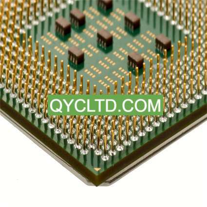
Coreless FC-BGA Package Substrates Manufacturer.As a leading Coreless FC-BGA Package Substrates manufacturer, we specialize in innovative and high-performance solutions for advanced electronic applications. Our cutting-edge technology and expertise ensure superior quality, high-density interconnections, and enhanced thermal management. We are committed to delivering reliable and cost-effective substrates that meet the evolving needs of the semiconductor industry.
Coreless FC-BGA (Flip Chip Ball Grid Array) package ركائز represent a significant advancement in semiconductor packaging technology. These substrates eliminate the conventional core layer found in traditional FC-BGA substrates, allowing for enhanced electrical performance, reduced package thickness, and improved thermal management. This article delves into the properties, structure, materials, manufacturing processes, applications, advantages, and frequently asked questions (FAQs) related to coreless FC-BGA package substrates.
Structure of Coreless FC-BGA Package Substrates
The structure of coreless FC-BGA package substrates is designed to maximize performance and minimize physical dimensions:
The substrate is made from high-performance materials such as BT (Bismaleimide-Triazine) resin or ABF (Ajinomoto Build-up Film) without the traditional core layer. This approach reduces overall thickness and enhances flexibility.

Coreless FC-BGA Package Substrates Manufacturer
Multiple layers of copper traces are used for electrical connections. These layers are finely patterned to achieve high-density interconnects necessary for advanced semiconductor devices.
High-performance dielectric materials with low dielectric constants and loss tangents are used to separate conductive layers. These materials ensure minimal signal loss and maintain signal integrity.
Microvias and through-hole vias are utilized to connect different layers of the substrate. Microvias, in particular, enable high-density routing and minimize parasitic inductance and capacitance.
Various surface finishes, such as ENIG (Electroless Nickel Immersion Gold) or OSP (Organic Solderability Preservatives), are applied to protect copper surfaces and enhance solderability.
The semiconductor die is encapsulated using materials that provide mechanical protection and thermal stability, ensuring reliable performance in various operating conditions.
Materials Used in Coreless FC-BGA Package Substrates
Key materials used in coreless FC-BGA package substrates include:
Known for its excellent thermal and mechanical properties, BT resin is a common choice for high-reliability applications.
This epoxy resin film offers excellent electrical insulation, high glass transition temperature, and good adhesion to copper.
High-purity copper is used for conductive traces due to its superior electrical conductivity and reliability.
Low dielectric constant and low loss tangent materials are essential for maintaining high signal integrity and minimal signal loss.
Surface finishes like ENIG and OSP are used to protect the copper traces from oxidation and enhance solderability.
Manufacturing Process of Coreless FC-BGA Package Substrates
The manufacturing process for coreless FC-BGA package substrates involves several precise steps to ensure high performance and reliability:
Choosing appropriate base materials and conductive layers based on performance requirements.
Building up multiple layers of conductive and dielectric materials without a core layer, forming a stable substrate with reduced thickness.
Precision drilling, including laser drilling, is used to create microvias and through-holes for vertical interconnections.
Electroplating copper onto the substrate and inside vias to establish reliable electrical connections.
Using photolithography and chemical etching to define the circuit patterns and interconnects.
Applying protective coatings to exposed copper surfaces to enhance solderability and protect against oxidation.
Attaching the semiconductor die to the substrate using advanced flip-chip bonding techniques, ensuring minimal signal loss and distortion.
Encapsulating the die for mechanical protection and thermal stability, followed by rigorous testing for electrical performance, سلامة الإشارة, and adherence to design specifications.
Applications of Coreless FC-BGA Package Substrates
Coreless FC-BGA package substrates are used in a wide range of high-performance applications, منها:
Smartphones, اقراص, and other portable devices that require compact and high-performance IC packaging.
Base stations, معدات الشبكات, and other communication devices that demand high-frequency signal transmission and reliable connections.
Advanced driver-assistance systems (ADAS), infotainment systems, and other electronic components in vehicles.
High-performance computing and control systems used in manufacturing and process automation.
Diagnostic and imaging equipment that require high reliability and precision.
Advantages of Coreless FC-BGA Package Substrates
Coreless FC-BGA package substrates offer several significant advantages:
Eliminating the core layer reduces the overall thickness of the package, enabling thinner and more compact device designs.
The absence of a core layer minimizes parasitic inductance and capacitance, improving signal integrity and reducing signal loss.
Better heat dissipation through the substrate materials and design features, ensuring stable operation under high-power conditions.
Supports complex and high-density routing, enabling advanced semiconductor designs.
The coreless design offers greater flexibility in substrate manufacturing and design, allowing for customized solutions.
الأسئلة المتداولة
What materials are typically used for coreless FC-BGA package substrates, and why?
Coreless FC-BGA package substrates commonly use materials like BT resin and ABF for their excellent thermal stability, القوة الميكانيكية, and electrical insulation properties. These materials are essential for maintaining reliability and performance in high-density and high-speed applications.
How do coreless FC-BGA package substrates differ from traditional FC-BGA substrates?
Coreless FC-BGA package substrates eliminate the core layer found in traditional FC-BGA substrates, resulting in reduced package thickness, enhanced electrical performance, and improved thermal management. This coreless design also allows for higher density interconnections and greater design flexibility.
What industries benefit the most from the use of coreless FC-BGA package substrates?
Industries such as consumer electronics, الاتصالات السلكيه, إلكترونيات السيارات, industrial automation, and medical devices benefit significantly from the use of coreless FC-BGA package substrates due to their reduced thickness, enhanced electrical performance, and improved thermal management.
How are coreless FC-BGA package substrates tested to ensure reliability?
Coreless FC-BGA package substrates undergo rigorous testing processes, including electrical testing for signal integrity and performance, ركوب الدراجات الحرارية, and reliability testing. These tests ensure that the substrates meet stringent performance and durability standards required for high-performance applications.
 الشركة المصنعة لحزمة أشباه الموصلات الركيزة