 반도체 패키지 기판 제조업체
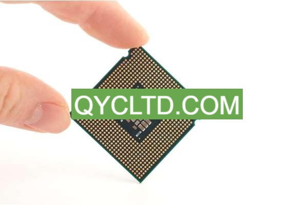
What is LCC Package Substrate?
LCC Package Substrate Manufacturer.LCC Package Substrate Manufacturer is a leading provider specializing in the production of high-quality leadless chip carrier (LCC (LCC)) substrates. These substrates are crucial for the efficient functioning of modern electronic devices, offering enhanced thermal management and electrical performance. The manufacturer utilizes advanced materials and cutting-edge fabrication techniques to ensure reliability and precision in their products, catering to the demands of the semiconductor industry and contributing to the advancement of miniaturized, high-performance electronics.
LCC (LCC) (무연 칩 캐리어) 포장 기판 is a commonly used integrated circuit (IC) 패키징 기술. It’s usually made from a rigid substrate covered with a metal layer that connects to the chip’s pins. Compared with the traditional DIP (dual in-line package), the LCC package is more compact and easier to install on the PCB. A distinctive feature of the LCC package is that its pins are lead-free, which complies with environmental standards and helps reduce negative impact on the environment. 또한, LCC packaging also has good thermal and electrical properties and is suitable for a variety of application scenarios, such as communications, automotive electronics, industrial control, 등. 일반 사항, LCC packaging substrate is an advanced and environmentally friendly IC packaging technology with broad application prospects.

LCC 패키지 기판 제조업체
LCC Package Substrate design Reference Guide.
LCC Package Substrate Design Reference Guide
LCC packaging substrate is a substrate type commonly used for integrated circuit packaging, and its design and manufacturing are of great significance in the electronics industry. This guide is intended to provide a reference for the design of LCC packaging substrates and covers the following main contents:
What is the LCC packaging substrate?
LCC packaging substrate is a substrate used for integrated circuit packaging, usually made of ceramic materials, to support and connect circuit components inside the chip.
What materials are used for LCC packaging substrates?
LCC packaging substrates usually use ceramic materials, such as aluminum oxide (Alumina) or boron nitride (Boron Nitride), to provide good thermal conductivity and electrical insulation.
What are the dimensions of the LCC package substrate?
The size of the LCC packaging substrate can vary depending on the specific application needs, and is typically found in square or rectangular forms with dimensions ranging from a few millimeters to tens of millimeters.
What is the manufacturing process of LCC packaging substrate?
The manufacturing process of LCC packaging substrates involves multiple steps, including raw material preparation, 금형 성형, 인쇄 회로, 소 결, 금속화 및 테스트.
What are the application fields of LCC packaging substrates?
LCC packaging substrates are widely used in the packaging of high-performance integrated circuits, especially in situations where good thermal conductivity and electrical performance are required, such as communication equipment, automotive electronics, and industrial control.
What are the advantages of LCC packaging substrates?
LCC packaging substrate has good thermal conductivity, excellent dimensional stability and good electrical insulation properties, and can meet the needs of high-performance integrated circuit packaging.
Frequently Asked Questions (자주 묻는 질문(FAQ))
This guide also includes answers to some frequently asked questions about LCC packaging substrate design and application to help readers better understand and apply this technology.
Through this guide, you can learn the basic knowledge about LCC packaging substrate design, as well as its applications and advantages in the electronics industry, helping you better apply this technology for integrated circuit packaging design.
What material is used in LCC Package Substrate?
LCC (LCC) (무연 칩 캐리어) packaging substrates are usually made of a variety of materials to meet their requirements in electronic devices. These materials must have excellent thermal conductivity, electrical insulation, and mechanical strength to ensure device performance and reliability. The following are some materials commonly used in LCC packaging substrates:
Organic substrate materials: Common organic substrate materials include FR-4 (glass fiber reinforced epoxy resin), FR-5 and BT (benzoquinonetriamine resin). These materials have good mechanical strength and electrical insulation properties, and are easily processed into desired shapes and sizes.
Metallization layer: LCC substrates usually have metallization layers that are used to connect chips and other devices. These metal layers are usually composed of copper, nickel plating and solder to provide good electrical conductivity and soldering properties.
Filling materials: In some high-end LCC packages, filling materials are used to fill cavities or gaps to improve the mechanical strength and thermal conductivity of the substrate. These filling materials are usually materials with good thermal conductivity, such as silicone or epoxy.
Pad material: The bottom of the LCC package usually has a pad for connection to the PCB (Printed Circuit Board). These pads are typically made from nickel, gold or tin alloys to provide good soldering performance and corrosion resistance.
Fillers: Some high-performance LCC packages may use fillers to fill the cavity to increase the strength and stability of the package. These fillers are usually non-conductive to avoid interfering with the circuitry inside the package.
일반 사항, the material selection for LCC packaging substrate depends on the required performance and application scenarios. Different material combinations can achieve different performance characteristics to meet the needs of various applications.
What size are LCC Package Substrate?
The size of ceramic packaging substrates varies depending on their purpose and application and is often determined by the size and requirements of the specific chip or device. 일반적으로 말하자면, ceramic packaging substrates can be square, rectangular or other shapes, and their dimensions can range from a few millimeters to tens of millimeters.
In the electronics industry, ceramic packaging substrates are usually used for packaging and connection of integrated circuits, 센서, microprocessors and other devices. Their size is often affected by the required circuit density, thermal management requirements, and space constraints of the specific application.
예를 들어, in some microelectronic devices, the ceramic packaging substrate may be only a few millimeters in size to accommodate miniaturization design needs. In some high-performance computer chips or other large electronic devices, the size of the ceramic packaging substrate may be larger to accommodate more circuits and connections.
일반 사항, the size of ceramic packaging substrates is determined based on specific design and application requirements and can vary greatly from case to case.
The Manufacturing Process of LCC Package Substrate.
LCC (LCC) (무연 칩 캐리어) packaging substrate is a type of substrate commonly used for integrated circuit packaging. Its manufacturing process includes multiple steps such as raw material preparation, mold molding, 인쇄 회로, 소 결, 금속화 및 테스트.
첫, the process of manufacturing LCC packaging substrates begins with the preparation of raw materials. This includes selecting the appropriate substrate material, usually fiberglass reinforced resin (FR-4) or other specific materials, and metallization materials such as copper foil. These raw materials must meet the requirements for strength, electrical conductivity and heat resistance required by the packaging substrate.
Next is the mold forming stage. 이 단계에서, the shape and size of the substrate will be manufactured by molding according to the design requirements. This may involve using processes such as machining or chemical etching to ensure precision and consistency of the substrate.
Then comes the process of printing the circuit. 이 단계에서, the surface of the substrate will be covered with conductive material through printing technology to form a circuit pattern. This is usually achieved by printing conductive ink or metallized film on the surface of the substrate and going through process steps such as photolithography and etching.
This is followed by the sintering stage. Once the circuit pattern is printed, the substrate is sent into a high-temperature baking oven for sintering. This step is designed to firmly bond the printed conductive material to the substrate surface, ensuring good electrical connection and stability.
Next comes the metallization process. 이 단계에서, the substrate’s metallization layer will be added to the printed circuit pattern to provide better conductivity and connectivity. This usually involves plating the circuit pattern with a layer of metal such as nickel, copper or gold to ensure good conductivity and reliability of the circuit.
드디어 테스트 단계가 시작됩니다. After completing all manufacturing steps, the LCC package substrate will be sent to the test equipment for functional and performance testing. These tests are designed to verify that the electrical connections to the substrate are functioning properly and that they meet design specifications and performance requirements.
일반 사항, the manufacturing process of LCC packaging substrates involves multiple key steps, including raw material preparation, 금형 성형, 인쇄 회로, 소 결, metallization, and testing. Each step is critical to the quality and performance of the final product. All have important impacts.
The Application area of LCC Package Substrate.
LCC (LCC) (무연 칩 캐리어) Packaging Substrate는 열전도율이 좋은 집적 회로 포장재입니다, 치수 안정성 및 전기 절연 특성. 고성능 집적 회로 패키징에서 중요한 역할을 하며 성능에 대한 엄격한 요구 사항을 충족합니다, 현대 전자 제품의 신뢰성과 안정성. 다음은 다양한 응용 분야에서 LCC 포장 기판의 구체적인 응용 분야입니다:
컴퓨터 및 서버에서, 고성능 프로세서 및 칩에 대한 패키징 요구 사항은 매우 엄격합니다. LCC 포장 기판은 우수한 열전도율을 제공할 수 있습니다, 효과적으로 열을 발산, and ensure the stability and reliability of the chip under high-load operating conditions. 동시에, 치수 안정성은 다양한 온도 조건에서 패키지의 안정성을 보장합니다, 장치의 성능과 수명을 향상시키는 데 도움이 됩니다..
통신 장비에서, LCC 패키징 기판은 무선 주파수와 같은 핵심 구성 요소의 패키징에 널리 사용됩니다 (무선 주파수 (RF)) 모듈 및 Baseband 프로세서. 우수한 전기 절연 특성은 RF 신호의 전송 품질을 보장합니다, 우수한 열전도율은 RF 모듈의 작동 온도를 낮추고 장비의 성능과 안정성을 향상시키는 데 도움이 됩니다.
자동차 전자 분야, LCC 패키징 기판은 차량 제어 장치와 같은 핵심 구성 요소를 패키징하는 데 사용됩니다 (ECU), 센서 및 드라이버. 치수 안정성과 전기 절연 특성은 자동차의 복잡한 작업 환경과 진동 조건에 적응할 수 있습니다, 전자 장비의 신뢰성과 내구성 보장.
산업 제어 및 자동화 시스템에서, LCC 패키징 기판은 PLC 패키징에 널리 사용됩니다. (프로그래밍 가능한 로직 컨트롤러), 센서, 액추에이터 및 기타 장비. 우수한 열전도율과 치수 안정성은 열악한 작업 환경에서 장비의 안정성과 신뢰성을 보장할 수 있습니다, 산업 생산 효율성 및 자동화 수준 향상.
소비자 가전 제품에서, 스마트 폰과 같은, 정제, 카메라, 등., LCC 패키징 기판은 고성능 프로세서 및 이미지 센서와 같은 핵심 구성 요소의 패키징에 널리 사용됩니다. 치수 안정성과 우수한 전기 절연 특성은 장비의 성능과 안정성을 향상시키고 소비자를 충족시키는 데 도움이 됩니다’ 제품 성능 및 경험에 대한 높은 요구 사항.
일반 사항, LCC 패키징 기판은 우수한 열전도율로 인해 고성능 집적 회로 패키징 분야에서 광범위한 응용 전망을 가지고 있습니다, 치수 안정성 및 전기 절연 특성, 성능을 충족시킬 수 있습니다., 다양한 분야의 전자 제품에 대한 신뢰성 및 안정성 요구 사항. 필요.
What are the advantages of LCC Package Substrate?
LCC (LCC) (무연 칩 캐리어) packaging substrate is a packaging solution with good thermal conductivity, 치수 안정성 및 전기 절연 특성. It is widely used in the packaging field of high-performance integrated circuits. Its advantages are mainly reflected in the following aspects:
좋은 열전도율: The LCC packaging substrate is made of high-quality thermal conductive materials, which can effectively conduct the heat generated by the chip and keep the chip within a safe operating temperature range. This helps improve the performance and stability of integrated circuits and reduces the risk of performance degradation or damage due to overheating.
Excellent dimensional stability: LCC packaging substrate has high dimensional stability and can maintain a stable packaging structure under different temperature and humidity conditions. This stability helps ensure the reliability of the connection between the chip and the external environment, reducing package failure or poor contact problems caused by temperature changes.
우수한 전기 절연 성능: The LCC packaging substrate is made of insulating materials, which can effectively block current transmission and provide good electrical insulation protection. This helps reduce the risk of crosstalk and electrical failures in the circuit, ensuring circuit stability and reliability.
Suitable for the packaging needs of high-performance integrated circuits: Because the LCC packaging substrate has good thermal conductivity, 치수 안정성 및 전기 절연 특성, it is very suitable for the packaging needs of high-performance integrated circuits. Whether in high-speed communications, computer processors or other fields, LCC packaging substrates can meet high requirements for packaging quality and performance stability.
요약하면 다음과 같습니다, LCC packaging substrates have become an ideal choice to meet the packaging needs of high-performance integrated circuits due to their good thermal conductivity, excellent dimensional stability and good electrical insulation properties. It plays an important role in improving the performance, stability and reliability of integrated circuits, and provides reliable packaging solutions for the development and application of electronic products.
자주 묻는 질문(FAQ)
What is an LCC package substrate?
An LCC (무연 칩 캐리어) package substrate is a type of electronic packaging used to mount and interconnect integrated circuits onto printed circuit boards (PCB (폴리염화비페닐)) or other substrates. It typically features a leadless design, meaning it lacks external leads protruding from the package body.
What are the advantages of using LCC package substrates?
LCC package substrates offer several advantages, including reduced footprint on PCBs, improved electrical performance due to shorter interconnection paths, enhanced thermal management, and compatibility with automated assembly processes.
How does an LCC package substrate differ from other packaging types?
Unlike traditional packages with external leads (such as dual in-line packages or quad flat packages), LCC package substrates have their leads positioned underneath the package body, allowing for a smaller footprint and better thermal dissipation.
What are the key considerations when designing with LCC package substrates?
Designers need to consider factors such as signal integrity, 열 관리, substrate materials, routing density, and manufacturing processes to ensure optimal performance and reliability when using LCC package substrates.
What types of applications are suitable for LCC package substrates?
LCC package substrates are commonly used in applications requiring high-density mounting of integrated circuits, such as mobile devices, networking equipment, automotive electronics, and industrial control systems.


