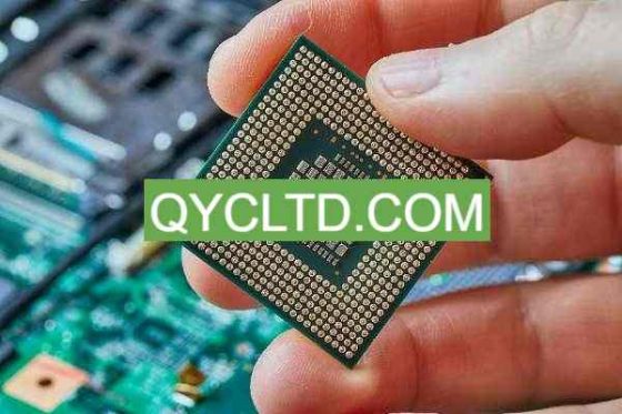
What is WLP Package Substrate?
WLP Package Substrate Manufacturer.A WLP (Wafer-Level Packaging) Package Substrate Manufacturer specializes in producing advanced substrates essential for semiconductor devices. These substrates are critical components that provide mechanical support and electrical connectivity for wafer-level packages, ensuring high performance and reliability in electronic products. Leveraging cutting-edge technology and precision engineering, these manufacturers play a crucial role in the electronics supply chain, supporting innovations in various industries, including consumer electronics, 自動車, and telecommunications.
WLP パッケージ基板 is an advanced packaging technology that has attracted much attention in the PCB industry today. This technology completes the packaging process at the wafer level, directly packaging IC chips on the wafer, and then cutting, testing and packaging. Compared with traditional packaging technologies, WLPパッケージ基板 has unique advantages, mainly reflected in its high integration and compact package size.
最初です, the core of WLP Package Substrate technology is packaging at the wafer level. This means that the IC chip completes the packaging process in the early stages of chip manufacturing, which can reduce subsequent packaging steps, improve manufacturing efficiency and reduce costs compared with traditional packaging technology. さらに, because the packaging process is completed at the wafer level, a higher level of integration can be achieved, making the overall package more compact, helping to reduce device size and improve device performance and reliability.
第二に, WLP Package Substrate has a smaller package size. Because the packaging process is done at the wafer level, smaller and thinner package sizes can be achieved. This makes WLP Package Substrate technology an important application prospect in the pursuit of miniaturization and lightweight electronic devices, such as smartphones, wearable devices and portable medical equipment. The small package size also helps reduce the PCB board footprint, providing designers with greater flexibility and freedom.

WLPパッケージ基板メーカー
最終的に, WLP Package Substrate technology can also achieve higher performance and lower power consumption. Since the packaging process is completed at the wafer level, the use of packaging materials can be reduced, thermal conduction and electrical losses can be reduced, and signal transmission speed and power consumption efficiency can be improved. さらに, WLP Package Substrate technology can also achieve better heat dissipation performance, allowing the chip to work at a lower temperature, extending the service life and stability of the device.
まとめると, WLP Package Substrate technology has broad application prospects and huge market potential. With the continuous development of electronic equipment and the intensification of miniaturization trends, it is believed that WLP Package Substrate technology will become a dazzling new star in the PCB industry, driving the industry forward and bringing a more convenient and intelligent life to mankind.
WLP Package Substrate design Reference Guide.
When designing the WLP Package Substrate, designers need to consider a variety of factors, which directly affect the performance and reliability of the final product. Here are some major design reference guidelines that designers need to fully understand and follow:
Wiring rules refer to the rules and principles for arranging wires, signal lines and power lines in PCB design. In WLP Package Substrate design, reasonable wiring rules can effectively reduce signal interference and crosstalk, and improve signal integrity and reliability. Designers need to rationally arrange wires and signal lines according to the characteristics and requirements of the circuit to avoid cross interference and power loss.
Signal integrity refers to maintaining signal integrity and stability during signal transmission. In the design of WLP Package Substrate, designers need to consider factors such as signal transmission rate, waveform shape, and electromagnetic interference, and adopt appropriate wiring schemes and signal processing technologies to ensure the stability and reliability of signal transmission.
Power consumption refers to the electrical energy consumed by a circuit during operation. In the WLP Package Substrate design, designers need to reasonably design the circuit structure and wiring scheme to reduce power consumption and improve the energy efficiency ratio and service life of the circuit. The use of low-power components and optimized circuit design can effectively reduce power consumption and extend battery life.
Heat dissipation refers to effectively transferring the heat generated in the circuit to the external environment to maintain the normal operating temperature of circuit components. In the WLP Package Substrate design, designers need to consider the heat dissipation design of the circuit, including the selection of heat dissipation structure and heat dissipation materials. Properly designing the heat dissipation structure and adding heat dissipation materials can effectively improve the heat dissipation efficiency of the circuit and ensure the stability and reliability of the circuit.
まとめると, designing WLP Package Substrate requires comprehensive consideration of multiple factors such as wiring rules, シグナルインテグリティ, power consumption, と熱放散. Designers need to fully understand the latest technologies and guidelines for PCB design, and take appropriate design solutions and optimization measures based on specific application requirements and design goals to ensure the performance and reliability of the design.
What material is used in WLP Package Substrate?
Material selection for WLP Package Substrate technology is one of the key factors in its success in achieving high performance and reliability. 通常, the materials used in WLP Package Substrate include substrate materials, metal layers, protective layers, 等. Each material plays an important role in the packaging process.
まずは, let’s look at the substrate material. The substrate material is the basis of WLP Package Substrate and carries chips and other packaging components. Commonly used substrate materials include silicon, glass, ceramics, and polymers. Among them, polymer materials such as polyimide (円周率) and polyamide (お父さん) are favored due to their excellent mechanical strength, thermal conductivity, and high temperature resistance. Selecting the appropriate substrate material ensures that the package remains stable and reliable under a variety of environmental conditions.
第二に, the metal layer plays the role of conduction and heat dissipation in the WLP Package Substrate. The metal layer is usually made of highly conductive materials such as copper, aluminum, gold or silver. These metal layers connect the chip to external circuits by forming wires and solder joints on the surface of the substrate. 同時に, the metal layer can also effectively conduct the heat generated by the chip to the external environment and keep the temperature of the package stable.
最終的に, the protective layer plays a role in protecting the chip and metal layer in the WLP Package Substrate. The protective layer is usually made of materials such as resin, epoxy resin or silicone, which can effectively prevent moisture, chemical substances and mechanical damage from damaging the package. Choosing the right protective layer material can extend the life of the package and improve its reliability.
原則として, the materials used in WLP Package Substrate need to have excellent thermal conductivity, electrical properties and mechanical strength to ensure the reliability and stability of the package. Reasonable selection and combination of these materials can enable WLP Package Substrate technology to perform well in various application scenarios and push the PCB industry to a higher level.
What size are WLP Package Substrate?
The size of the WLP Package Substrate is one of the key features of the technology and is typically very small, far smaller than what traditional packaging technologies can achieve. This small size design enables WLP Package Substrate to achieve higher integration and more compact packaging. As the requirements for volume and weight of electronic devices become more and more stringent, the size advantage of WLP Package Substrate has become an important factor in promoting its application.
最初です, the small size of WLP Package Substrate means that the chip package is more compact and can accommodate more functional units in a limited space. 従来の包装技術との比較, WLP Package Substrate can integrate more chips onto the same substrate, thereby achieving higher integration. This highly integrated design can not only save space on the PCB board, but also reduce the number of connection lines in the circuit, reduce the complexity of the circuit, and improve the reliability of the system.
第二に, the reduction in size also helps reduce the overall volume and weight of the device. In fields such as mobile communications and consumer electronics, it is very important to reduce the size and weight of equipment. The small size design of WLP Package Substrate makes mobile devices such as mobile phones and tablets thinner and lighter, and also provides the possibility for the development of emerging fields such as wearable devices and smart homes.
かつ, the size reduction helps improve performance and reliability. The small size design of WLP Package Substrate reduces the transmission distance between chips and components, thereby reducing signal transmission delay and power consumption. 同時に, the reduction in size also helps improve heat dissipation efficiency and reduce heat accumulation in the package, thereby improving system stability and reliability.
全, the small size design of WLP Package Substrate brings new possibilities to the development of electronic devices. It can not only achieve higher integration and more compact packaging, but also reduce the size and weight of equipment, improve performance and reliability, and inject new impetus into the innovation and development of electronic products.
The Manufacturing Process of WLP Package Substrate.
The manufacturing process of WLP Package Substrate is a precise and complex process involving multiple key steps, requiring strict process control and quality management to ensure the quality and performance of the final product.
The first is wafer processing. このステップの内容, silicon wafers are processed and processed using advanced semiconductor manufacturing techniques. This includes cleaning, photoresist coating, exposure, etching and other steps to form the necessary structures and patterns on the wafer surface.
Next comes metallization. A conductive metal layer is formed on the surface of the wafer by evaporating metal or using chemical deposition. This step is critical because it defines the way and structure of the circuit connections, which directly affects the electrical performance of the final product.
Then there’s encapsulation. このステップの内容, IC chips are packaged directly on the wafer. Through advanced packaging technology, including ball grid array (BGA) 包装, the chip is connected to the wafer surface, sealed and protected. This enables the chip to operate stably in the working environment and to be effectively connected to other circuit components.
Next comes testing. After the packaging is completed, it is crucial to rigorously test the WLP Package Substrate. This includes functional testing, reliability testing, performance testing, 等. to ensure that the product meets specifications and can operate reliably under a variety of operating conditions.
最終的に, there is encapsulation. After all testing is completed, the WLP Package Substrate is encapsulated in a final enclosure to protect it from environmental influences and physical damage. Encapsulation can also include steps such as labeling and packaging to facilitate subsequent transportation and use.
The entire manufacturing process requires strict process control and quality management. Failure in any link may lead to quality problems and performance degradation of the final product. そこで, manufacturers need to take a series of measures, including using advanced equipment and processes, implementing strict quality management systems, and conducting comprehensive product testing and verification, to ensure the production of high-quality WLP Package Substrate products.
The Application area of WLP Package Substrate.
As an advanced packaging technology, WLP Package Substrate’s application fields cover many industries, including mobile communications, consumer electronics, automotive electronics and industrial control. Its small size, high integration and low power consumption make it have broad development prospects in these fields.
In the field of mobile communications, with the popularity and increasing functions of mobile devices such as smartphones and tablets, higher requirements have been placed on packaging technology. Due to its small size and high integration, WLP Package Substrate can meet the size and performance requirements of mobile devices while achieving thinner, lighter and more efficient designs, thus promoting the advancement of mobile communication technology.
In the field of consumer electronics, WLP Package Substrate is widely used in consumer electronics products such as smart wearable devices, smart home products, and digital cameras. Its small size and high integration level not only enable refined product design, but also enhance product performance and functionality to meet consumers’ ever-increasing demands for product experience.
In the field of automotive electronics, with the development of automobile intelligence and electrification, the requirements for automotive electronic products are also constantly increasing. As an advanced packaging technology, WLP Package Substrate can achieve miniaturization, lightweight and high performance of automotive electronic products, while improving product reliability and durability, injecting new vitality into the development of the automotive electronics industry.
In the field of industrial control, the high integration and low power consumption of WLP Package Substrate make it an ideal choice for industrial control products. It can realize the compact design of the product, improve the performance and reliability of the product, while reducing the energy consumption and cost of the product, and meet the demand for efficient, stable and reliable products in the industrial control field.
原則として, WLPパッケージ基板, as an advanced packaging technology, has broad application prospects in the fields of mobile communications, consumer electronics, 自動車用電子機器, and industrial control. With the continuous advancement of technology and the continued growth of market demand, it is believed that WLP Package Substrate will play an increasingly important role in the future electronics industry and make greater contributions to the development of human society.
What are the advantages of WLP Package Substrate?
As an advanced packaging technology, WLPパッケージ基板 (Wafer Level Packaging Package Substrate) has shown many advantages in the PCB (Printed Circuit Board) industry. These advantages make it one of the popular technologies in the current PCB industry. The following are the main advantages of WLP Package Substrate over traditional packaging technologies:
The packaging size of WLP Package Substrate is usually very small, and because its packaging is completed at the wafer level, a more compact and compact packaging form can be achieved. This small-sized package allows electronic devices to achieve smaller designs, while also improving PCB layout flexibility and providing designers with more space to arrange other devices, thereby further improving the performance of the device.
WLP Package Substrate can achieve higher performance by optimizing the packaging structure and wiring design. Its packaging form reduces the signal transmission path, reduces the loss and delay of signal transmission, thereby improving the response speed and data transmission rate of the circuit. 同時に, WLP Package Substrate can also better control the signal integrity in the circuit, reduce the occurrence of signal interference and crosstalk, and improve the stability and reliability of the circuit.
Due to the small package size and short wiring of WLP Package Substrate, its power consumption is usually lower than traditional packaging technologies. The small-size package reduces the number of resistors, capacitors and other components in the circuit and reduces the power consumption of the circuit. 同時に, WLP Package Substrate can also better implement power consumption management and heat dissipation design, further improving the energy efficiency ratio of the circuit, extending battery life, and reducing device heating problems.
WLP Package Substrate improves circuit reliability by optimizing packaging materials and processes. Its packaging structure is more compact, can better resist the influence of the external environment, and improves the circuit’s resistance to vibration, impact and temperature changes. 同時に, WLP Package Substrate can also better control the heat distribution in the circuit, reduce the impact of thermal stress on the circuit, and extend the service life of the circuit.
まとめると, WLP Package Substrate has many advantages over traditional packaging technology, including small package size, high performance, low power consumption, and strong reliability. These advantages have made WLP Package Substrate one of the popular technologies in the current PCB industry, and it is widely used in mobile communications, consumer electronics, 自動車用電子機器, industrial control and other fields. With the continuous development of electronic equipment and the intensification of the trend of miniaturization, WLP Package Substrate technology will play an increasingly important role in the future.
FAQ
How is WLP Package Substrate technology different from traditional packaging technology?
従来の包装技術との比較, the biggest difference between WLP Package Substrate technology and WLP Package Substrate technology lies in the packaging method. Traditional packaging technology usually encapsulates the chip in a plastic or ceramic package after the chip is manufactured, while WLP Package Substrate technology completes packaging directly at the wafer level during the chip manufacturing process. This makes the WLP Package Substrate package more compact and highly integrated, while reducing the size and weight of the package.
Is the manufacturing process of WLP Package Substrate technology complicated?
The manufacturing process of WLP Package Substrate technology is indeed more complex than traditional packaging technology. Manufacturing WLP Package Substrate requires multiple processes, including wafer processing, metallization, 包装, testing and packaging. Each process requires strict process control and quality management to ensure the performance and reliability of the final product.
What application scenarios is WLP Package Substrate technology suitable for?
WLP Package Substrate technology is suitable for a variety of application scenarios, including mobile communications, consumer electronics, automotive electronics and industrial control. Its small size, high integration and low power consumption make it have broad application prospects in various application scenarios.
What are the advantages of WLP Package Substrate technology?
WLP Package Substrate technology has many advantages over traditional packaging technology. 最初です, its package size is smaller, which can achieve higher integration and more compact packaging form; secondly, it has higher performance, because the package is closer to the chip, reducing the signal transmission path, which can improve signal speed and reliability; again , lower power consumption, and more compact packaging also means shorter circuits, thereby reducing power consumption; finally, greater reliability, the packaging is closer to the chip, reducing external interference and losses, and improving overall reliability.
What is the future development trend of WLP Package Substrate technology?
The future development trend of WLP Package Substrate technology is mainly reflected in the continuous innovation and improvement of packaging technology. With the continuous development of electronic equipment and the intensification of the trend of miniaturization, WLP Package Substrate technology will become more and more important. More advanced packaging technologies may appear in the future to meet the growing demand for packaging performance of electronic equipment.
 半導体パッケージ基板メーカー
