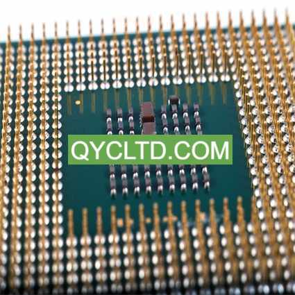
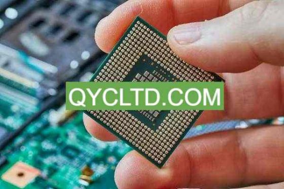
What is High Frequency Package Substrate?
High Frequency Package Substrate Manufacturer.A leading innovator in the realm of electronics, our company stands tall as a premier High Frequency Package Substrate Manufacturer. Pioneering cutting-edge technologies, we engineer substrates that enable high-speed data transmission, catering to the evolving demands of telecommunications, aerospaziale, and beyond. With meticulous attention to detail and a commitment to excellence, we craft substrates that embody reliability and performance, setting industry benchmarks. From concept to delivery, our relentless pursuit of perfection ensures that every substrate meets stringent quality standards, empowering our clients to unleash the full potential of their electronic systems with confidence and efficiency.
High-frequency substrato di imballaggio is a printed circuit board specially designed to handle high-frequency signals. They generally have higher dielectric constants, lower losses, and better signal transmission performance than traditional PCBs. These properties make high-frequency packaging substrates ideal for processing microwave and RF signals.
In the fields of high-frequency communications, radio frequency technology and microwave applications, stable and reliable signal transmission is crucial. The high-frequency packaging substrate is designed to meet this demand. They use special materials and processes to ensure optimal performance and reliability in high-frequency environments.
One of the key characteristics of high-frequency packaging substrates is their high dielectric constant. Dielectric constant refers to the material’s ability to respond to an electric field, and high-frequency packaging substrates usually use materials with higher dielectric constants, come il PTFE (Politetrafluoroetilene) or high-frequency ceramics, to enhance the signal transmission effect. This high dielectric constant allows signals to propagate quickly through the substrate, reducing signal delays and losses.
Inoltre, high-frequency packaging substrates also have lower signal losses. When processing high-frequency signals, signal loss will cause signal attenuation and distortion, reducing system performance. The high-frequency packaging substrate effectively reduces signal loss and maintains signal integrity and stability by optimizing material selection and design layout.
Another advantage of high-frequency packaging substrates is their good shielding properties. In high-frequency environments, electromagnetic interference may negatively impact system performance. The high-frequency packaging substrate adopts shielding design and ground wire layout, which effectively suppresses electromagnetic interference and ensures the stability and reliability of the system.

Produttore di substrati per pacchetti ad alta frequenza
Generalmente, high-frequency packaging substrates have obvious advantages when processing high-frequency signals, including high dielectric constant, low loss and good shielding performance. These advantages make high-frequency packaging substrates the first choice in wireless communications, radio frequency technology and microwave applications. With the continuous development of electronic technology, it is believed that high-frequency packaging substrates will continue to play an important role in future applications and promote innovation and progress in the electronic field.
High Frequency Package Substrate design Reference Guide.
Designing high-frequency packaging substrates is a complex task that requires the consideration of multiple factors to ensure that the final product meets the requirements of high-frequency applications. Here are some important things that are usually included in design guidelines:
Selezione del materiale: In the design of high-frequency packaging substrates, material selection is a crucial part. Different materials have different dielectric properties and loss factors, which directly affect the transmission performance of high-frequency signals. Design guides often provide an introduction to commonly used materials and their advantages and disadvantages in different application scenarios.
Wiring skills: The wiring of high-frequency circuits needs to consider factors such as signal integrity, Percorsi di trasmissione del segnale, and electromagnetic interference. The design guide provides routing techniques, including guidance on differential signal routing, Adattamento dell'impedenza, and signal and ground plane placement.
Ground wire design: The ground wire plays a vital role in high-frequency circuits, affecting the return path of signals and the suppression of electromagnetic interference. The design guide will introduce the design principles of ground wires in detail, including single-point grounding, layered grounding, and ground hole settings.
Shielding design: High-frequency circuits are often very sensitive to external interference, so effective shielding design is needed to protect the signal from interference. The design guide will introduce different types of shielding structures, such as metal casings, shielding cans, and underground shielding, as well as their design principles and application scenarios.
Simulation and verification: When designing high-frequency packaging substrates, simulation and verification work is usually required to ensure the feasibility and performance of the design solution. The design guide will introduce commonly used simulation tools and verification methods, such as SPICE simulation, electromagnetic field simulation, and experimental verification, to help engineers conduct design evaluation and optimization.
Application Examples: Finalmente, design guidelines often provide some practical application examples to demonstrate the effects and performance of different design solutions in specific applications. These examples can help engineers better understand design principles and provide reference for actual projects.
In sintesi, many factors need to be considered when designing high-frequency packaging substrates. The design guide provides comprehensive guidance from basic concepts to practical applications to help engineers overcome the challenges in high-frequency circuit design and achieve performance optimization and product reliability improvement. .
What material is used in High Frequency Package Substrate?
In the manufacturing of high-frequency packaging substrates, material selection is crucial because the electrical properties of the material directly affect the performance and stability of the entire system. High-frequency packaging substrates usually use special materials with excellent dielectric properties to meet the needs of high-frequency signal processing.
Among them, PTFE (Politetrafluoroetilene) is a commonly used high-frequency packaging substrate material. PTFE has extremely low dielectric loss and high dielectric constant, il che lo rende performante in ambienti ad alta frequenza. It also has excellent heat resistance and chemical stability, making it suitable for a variety of applications under high temperatures and harsh environments.
Another common material is FR-4 (fiberglass reinforced epoxy). FR-4 is a conventional printed circuit board substrate, but it can also be used for high-frequency packaging substrates after special treatment. It has good mechanical strength and dimensional stability, as well as appropriate dielectric properties to meet the needs of some medium-frequency high-frequency applications.
Inoltre, RO4003C is also a common high-frequency packaging substrate material. It is a glass fiber reinforced PTFE substrate with excellent dielectric properties and stability suitable for high frequency RF applications. RO4003C material has a low loss factor and consistent dielectric constant, providing reliable signal transmission performance.
These materials are widely used in high-frequency packaging substrates because they provide the required electrical properties and perform well in high-frequency environments. Engineers select the appropriate materials based on the requirements and performance needs of a specific application, combined with appropriate design and manufacturing processes to ensure the performance and reliability of the final product.
What size are High Frequency Package Substrate?
The size of the high-frequency packaging substrate is one of the crucial considerations in the design process. Tipicamente, these dimensions will vary based on the needs of the specific application to meet requirements such as equipment performance, space constraints, and operating environment. Below we take a closer look at the size range of high frequency packaging substrates and their use in different applications.
In many handheld devices, come gli smartphone, Compresse, and portable medical devices, high-frequency packaging substrates often require tiny dimensions. These devices often have severe space constraints, requiring compact and highly integrated circuit boards. High-frequency packaging substrates are designed to be small and lightweight in these applications to accommodate the trend of device miniaturization. These micro-package substrates often feature multi-layer designs to minimize space and increase circuit integration.
D'altra parte, in large-scale applications such as communication base stations, Sistemi radar, e comunicazioni satellitari, high-frequency packaging substrates often require larger sizes. These systems typically need to handle higher power signals and therefore require more space to accommodate complex circuits and components. Large package substrates can accommodate more functional modules, antennas and power circuits to meet the performance and reliability requirements of these applications. Inoltre, the large packaging substrate can also provide better heat dissipation to ensure stable operation for a long time.
In addition to size, the shape of the high-frequency packaging substrate may also vary depending on the application. Some special applications may require non-traditional shaped substrates, such as round, oval or odd-shaped substrates, to accommodate specific installation space or circuit layout needs.
Grembiule, high frequency package substrates come in a wide range of sizes, from tiny packages for portable devices to large packages for base stations and radar systems. This flexibility enables high-frequency packaging substrates to meet the needs of a variety of different applications, providing more choices and possibilities for the design and manufacturing of electronic devices.
The Manufacturing Process of High Frequency Package Substrate.
Manufacturing high-frequency packaging substrates is a complex and precise process involving multiple critical steps that requires strict control and high-quality equipment. These steps are detailed below:
High-frequency packaging substrates are usually produced from large sheets and need to be cut according to specific application requirements. The cutting process requires high-precision cutting equipment to ensure that the size and shape of the packaging substrate meet the design requirements.
Drilling holes in the package substrate is an important step in the manufacturing process. These holes are used to connect wires between different layers, mount components, or provide ventilation. Due to the particularity of high-frequency signals, the location and size of the drill holes must be precisely controlled to ensure that the performance of the circuit is not affected.
Chemical processing is one of the key steps in the process of manufacturing high-frequency packaging substrates. This includes surface preparation, dirt removal and metal deposition, and so on. Chemical treatment ensures the flatness and cleanliness of the packaging substrate surface for subsequent processing and assembly.
Copper plating is the final process step in manufacturing high-frequency packaging substrates. In this process, the surface of the packaging substrate is coated with a layer of copper for conductivity and protection. The thickness and uniformity of copper plating has a significant impact on the performance of the circuit and therefore requires precise control.
Manufacturing high-frequency packaging substrates requires high-precision equipment and strict process control. Any deviation or inconsistency may result in degraded or unstable performance of the circuit. Pertanto, manufacturers must invest considerable effort and resources to ensure the highest quality standards are met at every step.
The manufacturing process of high-frequency packaging substrates is a complex process that integrates multiple processes and requires precision equipment and strict control. Each step has a significant impact on the performance and reliability of the final product, so manufacturers must ensure that every detail is of the highest standard to meet customer needs and industry requirements.
The Application area of High Frequency Package Substrate.
As a key electronic component, high-frequency packaging substrate plays an important role in various fields. Its applications in wireless communications, Comunicazioni satellitari, Sistemi radar, medical equipment and aerospace are described in detail below.
In the field of wireless communications, high-frequency packaging substrates are widely used in mobile communications equipment, base stations, antenna systems and wireless network equipment. They can provide stable signal transmission and good anti-interference capabilities, providing support for high-speed data transmission and communication connections.
Le comunicazioni satellitari sono una parte importante del moderno campo delle comunicazioni, and high-frequency packaging substrates are an indispensable part of the satellite communications system. They are used in key components such as satellite transmitters, receivers, power amplifiers and modems to ensure the stability and reliability of satellite communication systems.
Nei sistemi radar, high-frequency packaging substrates are used to manufacture key components such as antenna arrays, signal processors, radio frequency modules and control units. They are able to provide highly integrated solutions to achieve high performance and accuracy in radar systems.
Nel campo delle apparecchiature mediche, high-frequency packaging substrates are widely used in medical imaging equipment, vital sign monitoring equipment and medical communication systems. They provide reliable signal processing and data transmission capabilities to support medical diagnosis and treatment.
Nel settore aerospaziale, high-frequency packaging substrates are used in avionics, spacecraft communication systems, navigation systems and radar systems. They are resistant to extreme environmental conditions and vibrations, ensuring stable operation and reliability of aerospace equipment.
High-frequency packaging substrates play an irreplaceable role in fields such as wireless communications, Comunicazioni satellitari, Sistemi radar, Attrezzature mediche, and aerospace. They support the performance and reliability of equipment and drive the development and advancement of modern electronic technology. With the continuous advancement of technology and the expansion of application fields, high-frequency packaging substrates will continue to play an important role in providing long-lasting electronic solutions for various application scenarios.
What are the advantages of High Frequency Package Substrate?
High-frequency packaging substrates have attracted much attention in the field of modern electronics, and their outstanding advantages make them the first choice for processing high-frequency signals. Rispetto al PCB tradizionale, high-frequency packaging substrate has the following significant advantages:
Minore perdita di segnale: The high-frequency packaging substrate uses high-quality materials and precise manufacturing processes, which greatly reduces signal loss during transmission. This means that in long-distance transmission and high-frequency applications, signals can be transmitted more stably without distortion or attenuation due to loss.
Better signal integrity: Signal integrity is maintained due to the precision design and excellent electrical performance of the high-frequency packaging substrate. This means the signal is not subject to interference or distortion, ensuring system performance and stability. This advantage is especially important in applications that require high precision and reliability.
Higher reliability: High-frequency packaging substrates undergo strict quality control and testing, resulting in higher reliability. Its material selection and manufacturing process have been carefully designed to ensure stable performance in a variety of environmental conditions. This makes high-frequency packaging substrates ideal for many critical applications, including military, aerospace and medical devices.
Suitable for various harsh application scenarios: The excellent performance of high-frequency packaging substrates makes it widely used in various harsh application scenarios. High-frequency packaging substrates can perform well whether in extreme temperature, humidity or vibration environments, or in situations where high-frequency noise interference is significant. This makes them an integral part of many key industries.
In sintesi, high-frequency packaging substrates have become an important part of the modern electronics field due to their low signal loss, good signal integrity, high reliability and strong applicability. They not only provide stable performance when processing high-frequency signals, but also provide reliable solutions for a variety of demanding application scenarios. With the continuous development and innovation of technology, it is believed that high-frequency packaging substrates will continue to play an important role and promote the progress and development of the electronic field.
Domande frequenti
What is the difference between high-frequency packaging substrate and ordinary PCB?
High-frequency packaging substrates typically have higher dielectric constants and lower signal losses, allowing them to handle high-frequency signals more efficiently. Inoltre, high-frequency packaging substrates are often made of special materials to meet the requirements of high-frequency applications, while ordinary PCBs may not be able to meet these requirements.
How to choose a suitable high-frequency packaging substrate material?
Material selection depends on the requirements of the specific application. Generale, factors such as dielectric constant, loss factor, thermal stability, and cost need to be considered. PTFE (Politetrafluoroetilene) is typically used for high-performance applications, while FR-4 (fiberglass-reinforced epoxy) may be better suited for applications with lower general performance requirements.
What are the key steps in the manufacturing process of high-frequency packaging substrates?
Key steps include material preparation, printing, chemical processing, trivellazione, copper plating, patterning, soldering, assembly and testing, and so on. Each step requires precise control and high-quality equipment to ensure the performance and reliability of the final product.
How to deal with EMI (Electromagnetic Interference, electromagnetic interference) in high-frequency packaging substrates?
High-frequency packaging substrates usually use good grounding and shielding designs to reduce the impact of electromagnetic interference. Inoltre, choosing the right materials and wiring techniques can also help reduce electromagnetic interference.
What application fields are high-frequency packaging substrates suitable for?
High-frequency packaging substrates are widely used in wireless communications, Comunicazioni satellitari, Sistemi radar, Attrezzature mediche, aerospaziale e altri settori. They play a critical role in these applications, supporting equipment performance and reliability.
 Pacchetto Semiconduttore Substrato Fornitore
